ET-3200 Digital Trainer · Volume 2
How It Works
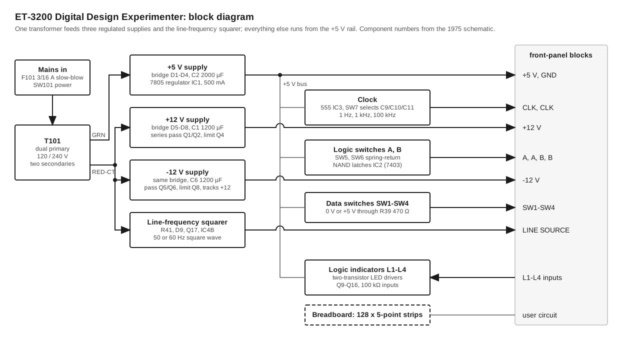
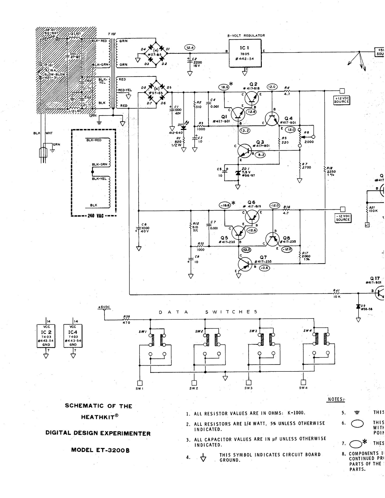
The ET-3200 contains no logic of its own beyond two quad NAND gates and a 555 timer. Its job is to support the student’s circuit. It supplies clean power at three voltages, defined logic levels on eight input terminals (four data and four latched logic outputs), a clock, a mains-locked reference frequency, and four indicators that show a logic level without loading the circuit that drives them. This volume follows the 1975 schematic stage by stage, then notes what changed in the ET-3200B of 1983. Component numbers are Heath’s. Voltages in brackets are the values printed in circles on the schematic, measured by Heath with a high-impedance voltmeter.
2.1 The circuit in one page
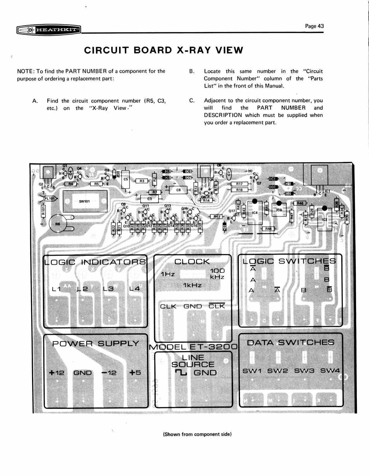
The whole instrument is on one printed board, part 85-1599, laid out so that its lower two-thirds forms the silk-screened front panel. There are five functional groups:
- Power supplies: +5 V at 500 mA for logic, and ±12 V at 100 mA each for linear circuits, op-amps, MOS devices and interface experiments.
- Data switches SW1–SW4: static 0 or 1 sources.
- Logic switches A and B: spring-return switches with debounce latches, giving clean single transitions and complementary outputs.
- Clock and line source: a 555 astable at three frequencies with complementary outputs, and a mains-derived square wave.
- Logic indicators L1–L4: LED drivers with a high-impedance input.
Heath’s own Circuit Description in the manual runs to one page (ET-3200 manual, p. 42). The walk-through below expands it from the schematic.
2.2 Mains input and transformer
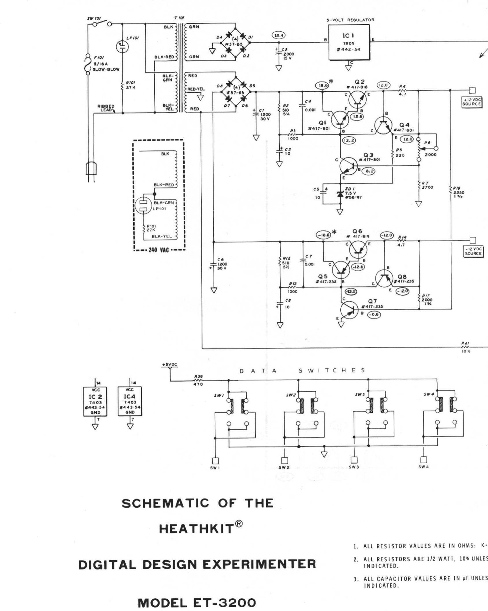
The line cord of the original ET-3200 is two-wire. It feeds a 3/16-ampere slow-blow fuse in clips (F101), the rocker power switch SW101, and the primary of the transformer T101 (Heath 54-893). The primary is split into two windings. For 120 V they are connected in parallel and for 240 V in series. The kit builder chooses one of two wiring diagrams at assembly (manual, “Alternate Line Voltage Wiring”, p. 23). A neon lamp (LP101) with a 27 kΩ series resistor (R101) sits across the 120 V winding as the pilot light and is visible through a red lens at the upper left of the panel.
There are two secondaries. A green winding feeds the +5 V supply alone. A red winding with a red-yellow centre tap feeds both 12-volt supplies and, through a 10 kΩ resistor, the line-frequency squarer.
2.3 The +5 V supply
The green winding feeds a bridge of four 1N4002 diodes (D1–D4) and a 2000 µF, 15 V electrolytic (C2), giving about 12.4 V unregulated. A 7805 three-terminal regulator (IC1, Heath 442-54) brings this down to +5 V. The regulator bolts to the board with a large heat sink and silicone grease. The manual specifies 500 mA with “thermal overload protection”, which is the 7805’s own internal shutdown.
The margin is generous for a 5-volt regulator. At the full 500 mA the 7805 drops about 7.4 V and dissipates about 3.7 W, which is why it gets the largest heat sink in the kit. The price is heat. The trainer warms up noticeably with a full breadboard of standard TTL, and the regulator is the component most worth checking in an old unit (see volume 6).
2.4 The ±12 V supplies
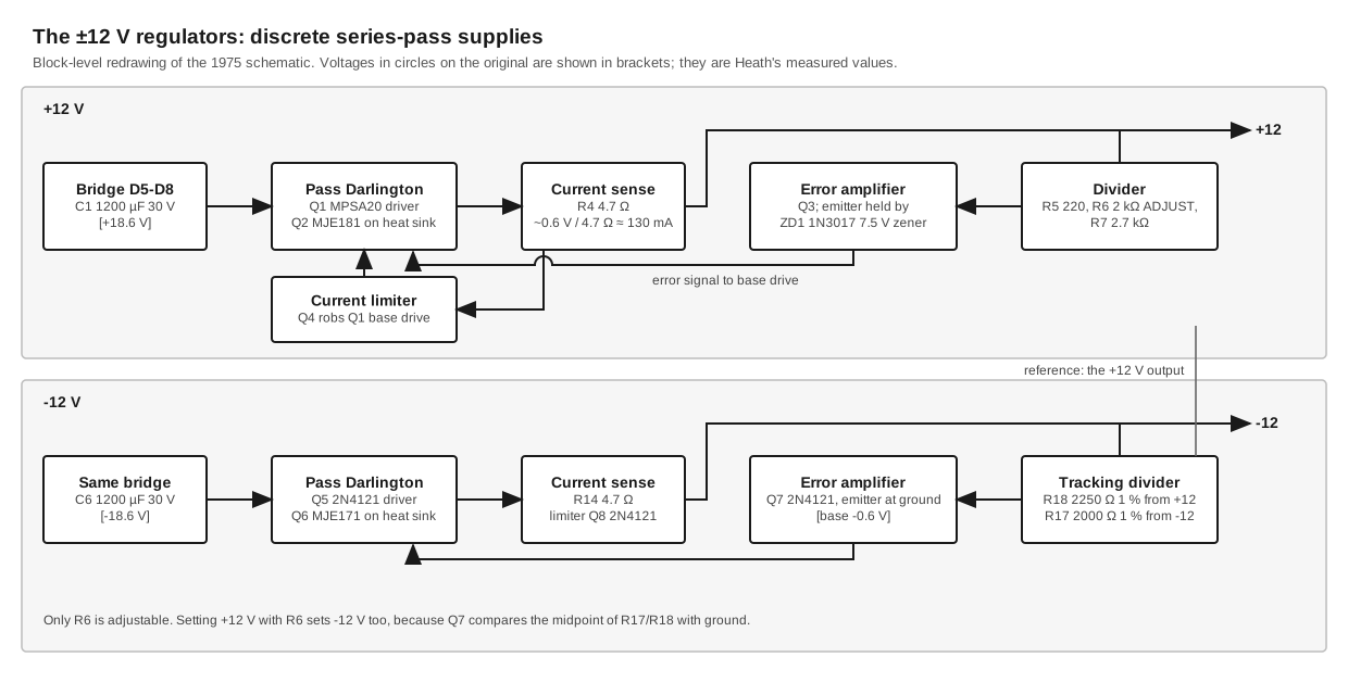
The ±12 V rails are regulated by discrete transistors rather than an IC. The red winding and a second bridge (D5–D8, 1N4002) give +18.6 V and −18.6 V about the centre tap, filtered by C1 and C6 (1200 µF, 30 V each).
Positive side. Q2, an MJE181 NPN power transistor (Heath 417-818) on a small heat sink, is the series pass element. Q1 (MPSA20) drives it as a Darlington pair, with base current supplied through R2 (510 Ω) from the unregulated rail. Q3 is the error amplifier. Its emitter is held at 7.5 V by the zener ZD1 (1N3017), and its base [8.2 V] is fed from the divider R5, R6 (the 2 kΩ VOLTAGE ADJUST control) and R7 across the output. If the output rises, Q3 conducts harder, pulls down Q1’s base [13.2 V] and throttles Q2.
A second transistor, Q4, provides current limiting. The load current flows through R4, a 4.7 Ω resistor. When the drop across it reaches a base-emitter voltage, about 0.6 V or 130 mA, Q4 turns on and diverts Q1’s base current. The manual puts it plainly: “the current is limited to a safe value” (manual, p. 42). That is why a student’s short circuit from +12 V to ground does no harm.
Negative side. The negative regulator mirrors the positive one with PNP parts: Q6 (MJE171, Heath 417-819) as pass transistor, and 2N4121s as driver (Q5), current limiter (Q8, with R14 4.7 Ω) and error amplifier (Q7). It has no zener of its own. Q7’s emitter is grounded and its base sits at the junction of two 1 % precision resistors: R18 (2250 Ω) from the +12 V output and R17 (2000 Ω) from the −12 V output. Q7 keeps that junction at about −0.6 V, so the negative output tracks the positive one. As the manual says, “the positive 12-volt supply is used as the reference for the negative 12-volt supply.” Setting +12 V with R6 during the test procedure sets −12 V automatically. That is the only adjustment in the kit.
The discrete design is modest by the standards of 1975, when IC regulators such as the 723 were cheap. Heath gave no reason for it. The ET-3100’s variable supplies were also discrete and current-limited, with 4.7 Ω limit resistors until the ET-3100B reduced them to 1.8 Ω (Eckweiler #129), which suggests shared engineering between the two trainers. The Troubleshooting Chart lists the likely failures: “both plus and minus 12-volt supplies are high and will not adjust” points to Q3 open or Q1 or Q2 shorted; “−12-volt supply is high; +12-volt supply is OK” points to Q7 open or Q5 or Q6 shorted (manual, p. 40).
2.5 Data switches
The four data switches (SW1–SW4) are DPDT slide switches wired as single-pole changeovers. In the down position the output terminal is connected straight to ground. In the up position it is connected to +5 V through R39, a single 470 Ω resistor shared by all four switches (schematic). The Circuit Description says only that “Resistor R39 limits the current.”
The shared resistor explains the specification of 10 mA maximum per switch, since 5 V across 470 Ω is 10.6 mA into a short. It also has a consequence the manual does not mention. Every switch set to 1 draws its load current through the same resistor, so heavily loaded high switches pull each other down. With TTL loads (40 µA per input when high) this does not matter. With a discrete transistor or an LED as the load, it does. The Digital Techniques course turned this into a design exercise. Experiment 1 of the EE-3201A text has the student design a saturated transistor switch driven from SW1, with “+5 volts as seen through a 470 Ω resistor”, and include R39 in the base-current calculation (EE-3201A textbook, pp. 2-38 to 2-39).
2.6 Logic switches: the debounce latch
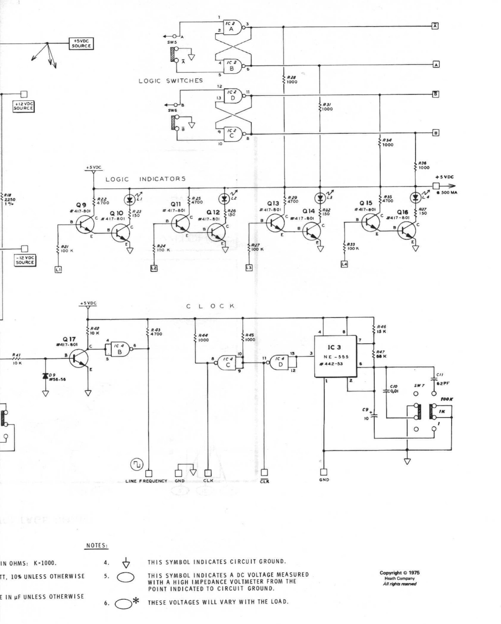
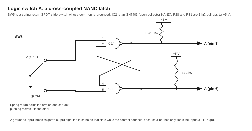
A mechanical switch contact bounces for a few milliseconds when it closes. A counter fed directly from such a switch counts each bounce. The ET-3200’s two logic switches, labelled A and B on the panel, are there to provide one clean edge per push. Each is a spring-return SPDT slide switch (SW5, SW6) whose common is grounded, feeding an R-S latch made of two cross-coupled NAND gates in IC2, an SN7403 quad two-input NAND.
In the rest position the switch grounds one latch input; pushing it grounds the other. Grounding a NAND input forces that gate’s output high, and the cross-coupling holds the latch in that state. When the contact bounces, the input merely floats for a moment. A floating TTL input reads as high, which leaves the latch where it is. The Circuit Description walks through the gate states pin by pin (manual, p. 42).
The 7403 is an open-collector part, so each output (A, Ā, B, B̄) has its own 1 kΩ pull-up to +5 V (R28, R31, R34, R36). The specification gives the output states as “+5 volts and +0.2 volts”. The high level is therefore a resistive 5 V, not a totem-pole output. A 1 kΩ pull-up will drive many TTL inputs, and it also lets the outputs work with CMOS running at 5 V.
2.7 Logic indicators
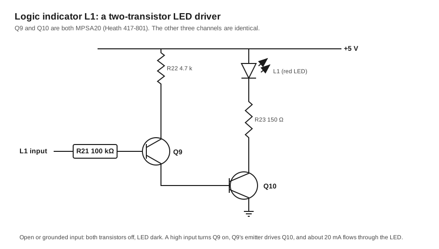
Each of the four indicators is a two-transistor switch driving a red LED. For channel L1: the input terminal feeds the base of Q9 (MPSA20) through R21, 100 kΩ. Q9’s collector goes to +5 V through R22 (4.7 kΩ), and its emitter drives the base of Q10. Q10 sinks the LED current through R23 (150 Ω). With a high input both transistors conduct, and about 20 mA flows through the LED. With the input open or grounded both are off and the LED is dark (manual, p. 42).
Two properties matter for teaching. The first is load. At +5 V input the 100 kΩ resistor admits less than 40 µA, about one TTL high-level input load, so an indicator can be clipped onto any node without changing the circuit’s behaviour. The second is threshold. The indicator lights when the input exceeds two base-emitter drops plus the drop across R21, roughly 1.3–1.5 V. That falls inside TTL’s undefined band (0.8 to 2.0 V). An indicator therefore shows a solid TTL high or low correctly, but it is not a logic probe and will not flag a marginal level. The EE-3201A text tells students that the inverter symbol it draws in front of each LED “represents the internal LED driver circuit and not an external inverter”, and that “when the input is open or grounded, the LED is off” (EE-3201A textbook, p. 3-35).
2.8 Clock
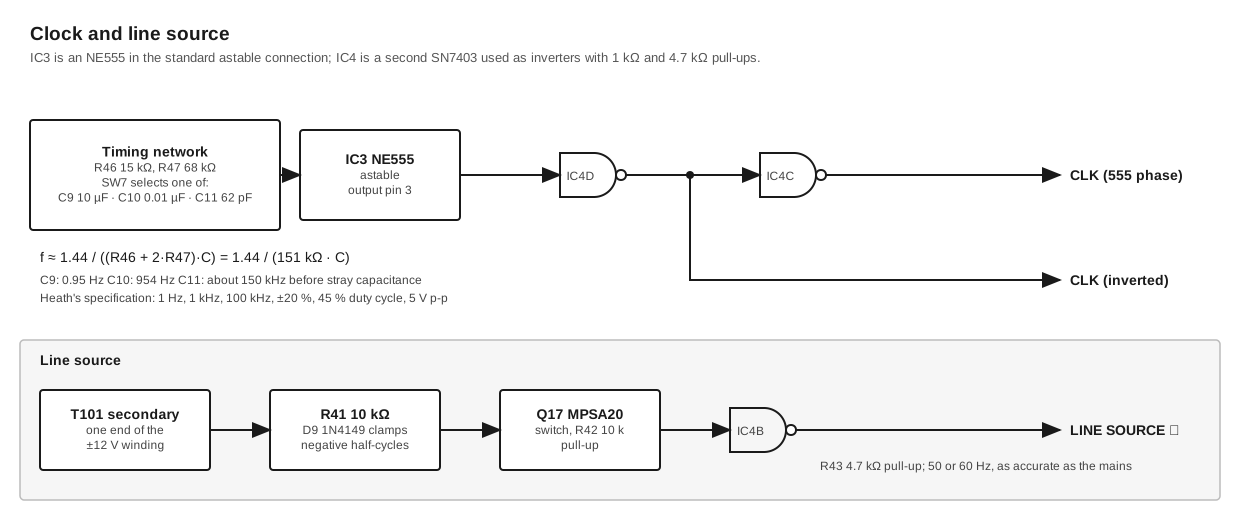
The clock is an NE555 (IC3, Heath 442-53) in the standard astable connection. R46 (15 kΩ) and R47 (68 kΩ) set the charge and discharge paths, and the three-position slide switch SW7 selects the timing capacitor: C9 (10 µF tantalum), C10 (0.01 µF Mylar) or C11 (62 pF mica). The 555’s output (pin 3) drives one NAND gate of IC4 (a second SN7403) wired as an inverter, which gives CLK̄. A second inverter restores the original phase as CLK. Both have 1 kΩ pull-ups (R44, R45), and both outputs are 5 V peak-to-peak.
The textbook 555 formula gives the frequencies: f ≈ 1.44 / ((R46 + 2·R47)·C) = 1.44 / (151 kΩ · C). That works out to 0.95 Hz with C9 and 954 Hz with C10, very close to the nominal 1 Hz and 1 kHz. With C11 the formula gives about 150 kHz. The specified 100 kHz is reached because the 62 pF capacitor is small enough that the 555’s own pin capacitance and the wiring to SW7 add a substantial fraction to it. This explains the loose ±20 % tolerance. The same resistor pair gives a high time of (R46 + R47)/(R46 + 2·R47), about 55 % of the period, and a low time of about 45 %. The manual’s “duty cycle 45 %” is presumably measured on the low half or on CLK̄.
At 1 Hz a student can watch a counter step on the LEDs. At 1 kHz the LEDs appear continuously lit, which the test procedure uses as a check. At 100 kHz the clock is fast enough to show propagation effects on an oscilloscope.
2.9 Line-frequency source
The LINE SOURCE terminal gives a logic-level square wave at the mains frequency. One side of the red secondary drives the base of Q17 (MPSA20) through R41 (10 kΩ). D9, a 1N4149, clamps the negative half-cycles, so “the positive excursions turn on transistor Q17.” Q17’s collector has a 10 kΩ pull-up (R42) and drives the last gate of IC4, “connected as an inverter”, whose output has a 4.7 kΩ pull-up (R43) (manual, p. 42). The result is 60 Hz in North America and 50 Hz elsewhere. Its duty cycle is somewhat below 50 %, because Q17 turns on only after the half-cycle has risen past about 0.6 V. The long-term frequency accuracy is that of the power grid, which the manual gives as 0.1 %. Digital clocks of the period used the mains as their timebase in the same way, and the course used it as a known frequency for counters and dividers.
2.10 Interfacing to other logic families
The manual has a page and a half on “IC Logic Compatibility”. Its chart rates the trainer’s supplies, switches and indicators as directly compatible with TTL (including open-collector, Schottky and three-state types), CMOS on the +5 V supply, and nMOS where the part uses +5 V. Static pMOS is “TTL compatible, static types only”. Linear circuits are “good for op amps, line drivers and receivers” using the ±12 V supplies (manual, pp. 37–38).
Two families need help. For RTL, Figure 2 of the manual drops the +5 V rail to about +3.6 V through two silicon diodes and a 100 µF capacitor; the switches’ higher 1 level “will not damage RTL circuits”. For ECL, which normally runs from −5.2 V, the manual suggests running the chips from the +5 V supply upside down, “Connect the IC ground to +5 volts and the normal supply input (VEE) to ground”. It then gives transistor level-translator circuits (Figures 3 and 4, using an MPS3639 or 2N5771) to make ECL work with the trainer’s TTL-level switches and indicators. These pages are reproduced in volume 4.
2.11 What changed in the ET-3200B
The 1983 ET-3200B manual (595-2936-06) prints the same specifications and, apart from component numbering added for new parts, the same Circuit Description (ET-3200B manual, pp. 46–47). Comparing the two parts lists and assembly sections shows these changes:
Table 1 — The 1983 ET-3200B manual (595-2936-06) prints the same specifications and, apart from component numbering added for new parts, the same Circuit Description ([ET-3200B manual, pp. 46–47](https://archive.org/details/manualsplus11835)). Comparing the two parts lists and assembly sections shows these changes
| Area | ET-3200 (1975) | ET-3200B (1983) |
|---|---|---|
| Line cord | two-wire (smooth and ribbed leads) | three-wire, with the green lead to a ground lug |
| Mains filtering | none | toroid coil L101, 0.047 µF Mylar across the line (C101), two 0.001 µF discs to ground (C102, C103) |
| Fuse | 3/16 A slow-blow in clips inside the terminal-strip box | same rating in a panel fuseholder |
| Pilot lamp | neon PL101 with 27 kΩ | LED D11 with R1, 820 Ω ½ W |
| LED drivers | Q9, Q11, Q13, Q15 bases fed only through 100 kΩ | 150 kΩ resistors from each of those bases to ground added (R48, R49, R51, R52), fitted on the foil side |
| Filter capacitors | C1, C6 1200 µF; C2 2000 µF | C1, C6 1000 µF; C2 2200 µF |
| Resistors | ½ W, 10 % | ¼ W, 5 % |
| Circuit board | 85-1599-2 | 85-2572-3 |
| Labels | caution label | adds an “FCC Compliance label” |
The mains filter and FCC label follow from the Federal Communications Commission’s rules for “computing devices”, Part 15, Subpart J. Those rules, adopted in 1979 and phased in over the following years, covered any device that generated timing pulses faster than 10,000 per second and required it to be verified against emission limits; Class B was the stricter category for equipment used in homes. An ET-3200A in the blue cabinet carries a Heath label that certifies the equipment “can be expected to comply with the emission limits for a Class B computing device pursuant to Subpart J of Part 15 of the FCC rules when assembled in strict accordance with the instructions” (Next Day Automation listing, bottom-view photograph). The FCC changes therefore date from the A version, not the B. Whether the A also had the line filter, the LED pilot and the 150 kΩ resistors cannot be settled without an ET-3200A manual. None was found.
The added 150 kΩ resistors change the indicator slightly. With 100 kΩ in series and 150 kΩ to ground, an open input is held firmly off. A high input must now also feed the 150 kΩ resistor, and the extra current through the 100 kΩ series resistor raises the switching threshold by nearly a volt, to roughly 2.2 V. That is just above TTL’s 2.0 V minimum input-high level, so after the change a lit indicator means a valid TTL 1. The likely purpose was to stop an open input from glowing through leakage, or through the capacitive pickup that a long jumper wire can gather. The manual gives no reason. The ET-3200B manual also warns that its C101 capacitor “is rated for 120 VAC only” and must be replaced with a UL-rated 250 V part before the unit is wired for 240 V (ET-3200B manual, p. 25).
2.12 Semiconductor complement
Table 2 — Semiconductor complement
| Ref. | Type | Heath no. | Function |
|---|---|---|---|
| IC1 | µA7805 | 442-54 | +5 V regulator |
| IC2, IC4 | SN7403N | 443-54 | quad 2-input NAND, open collector: switch latches; clock and line-source inverters |
| IC3 | NE555V | 442-53 | clock |
| Q2 | MJE181 (NPN) | 417-818 | +12 V pass |
| Q6 | MJE171 (PNP) | 417-819 | −12 V pass |
| Q1, Q3, Q4, Q9–Q17 | MPSA20 (NPN) | 417-801 | drivers, error amp, limiter, LED drivers, line squarer |
| Q5, Q7, Q8 | 2N4121 (PNP) | 417-235 | −12 V driver, error amp, limiter |
| D1–D8 | 1N4002 | 57-65 | rectifier bridges |
| D9 | 1N4149 | 56-56 | line-source clamp |
| ZD1 | 1N3017 (7.5 V) | 56-97 | +12 V reference |
| L1–L4 | red LED | 412-611 | logic indicators (412-640 in the ET-3200B, which also uses one as pilot D11) |
Source: ET-3200 manual, Parts List, pp. 3–8; ET-3200B manual, Parts List.
Sources
- Heath Company. Heathkit Manual for the Digital Design Experimenter, Model ET-3200, 595-1740-03, © 1975: Circuit Description, Specifications, IC Logic Compatibility, Troubleshooting Chart. https://archive.org/details/Heathkit_ET-3200_Digital_Design_Experimenter
- Heath Company. ET-3200 illustration booklet with schematic, © 1975 (schematic) and 1976 (pictorials). https://archive.org/details/HeathkitET3200DigitalDesignExperimenterschematic · https://archive.org/details/heathkit_et-3200
- Heath Company. Heathkit Manual for the Digital Design Experimenter, Model ET-3200B, 595-2936-06, © 1983. https://archive.org/details/manualsplus_11835 ; illustration booklet https://archive.org/details/Heathkit_ET-3200B_Experimenter
- Heathkit Educational Systems. Digital Techniques (EE-3201A textbook), 595-2931-09. https://archive.org/details/ee-3201-a-digital-techniques-individual-learning-system-textbook-1998
- Eckweiler, Bob (AF6C). “Heathkit of the Month #129: Heathkit ET-3100/A/B.” https://www.w6ze.org/Heathkit/Heathkit_129_ET3100B.pdf
- Next Day Automation, sales listing SB-202541 (ET-3200A, FCC label photograph). https://www.nextdayautomation.com/products/used-heathkit-et-3200-a-digital-design-experimenter-laboratory-breadboard-120-240vac
Comments (0)