SB-102 Transceiver · Volume 2
How It Works
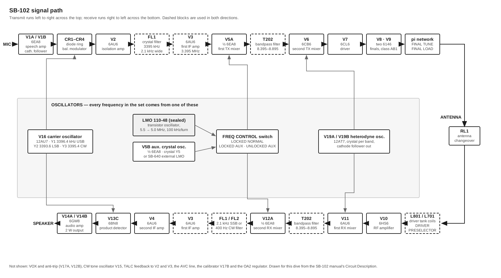
The SB-102 is a filter-type SSB transceiver of the classical pattern. The sideband is generated once, at a fixed low frequency where a crystal lattice filter can be sharp and cheap, then heterodyned up to the operating frequency in two steps; to receive, the whole chain runs backwards. Most of the chain is shared with the HW-101, which Heath derived from it, and the HW-101 dive’s circuit volume walks through the shared stages in detail. This volume covers the architecture once and then concentrates on what is particular to the SB-102: the sealed transistor Linear Master Oscillator and its supply, the FREQ CONTROL switching that the HW line never had, the Miller-effect correction in the driver, the receiver tube line-up, and the five-function metering.
Everything here is taken from the Circuit Description in the assembly manual (pages 135 to 155 of edition 595-1058-06) unless another source is named.
2.1 The frequency scheme
Four oscillators set every frequency in the set.
- The carrier oscillator, V16 (12AU7). Two Colpitts crystal oscillators share one envelope. V16A runs crystal Y1 at 3396.4 kHz for upper sideband; V16B runs Y2 at 3393.6 kHz for lower sideband or Y3 at 3395.4 kHz for CW transmit. Wafers of the MODE switch choose which half gets B+ and which crystal reaches the grid.
- The LMO. A sealed transistor oscillator, Heath part 110-48, tuning 5.0 to 5.5 MHz at 100 kHz per turn of the shaft. It is described in its own section below.
- The auxiliary crystal oscillator, V5B (half a 6EA8). A crystal-controlled Colpitts oscillator that can stand in for the LMO. Its crystal, Y5, plugs into a socket on the bandpass circuit board.
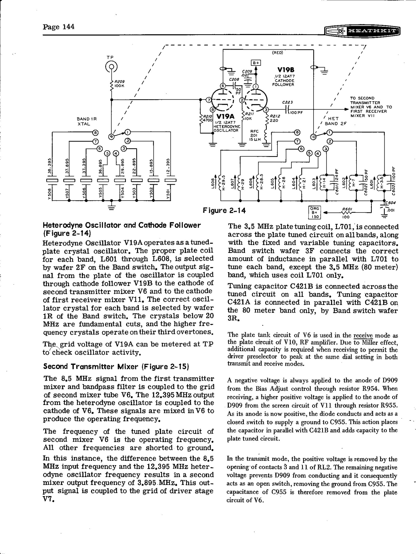
- The heterodyne oscillator, V19A (half a 12AT7). A tuned-plate crystal oscillator with one crystal and one plate coil per band. The crystals below 20 MHz are fundamental cuts; the higher ones run on their third overtones. V19B, the other half of the 12AT7, is a cathode follower that feeds both the second transmitter mixer and the first receiver mixer.
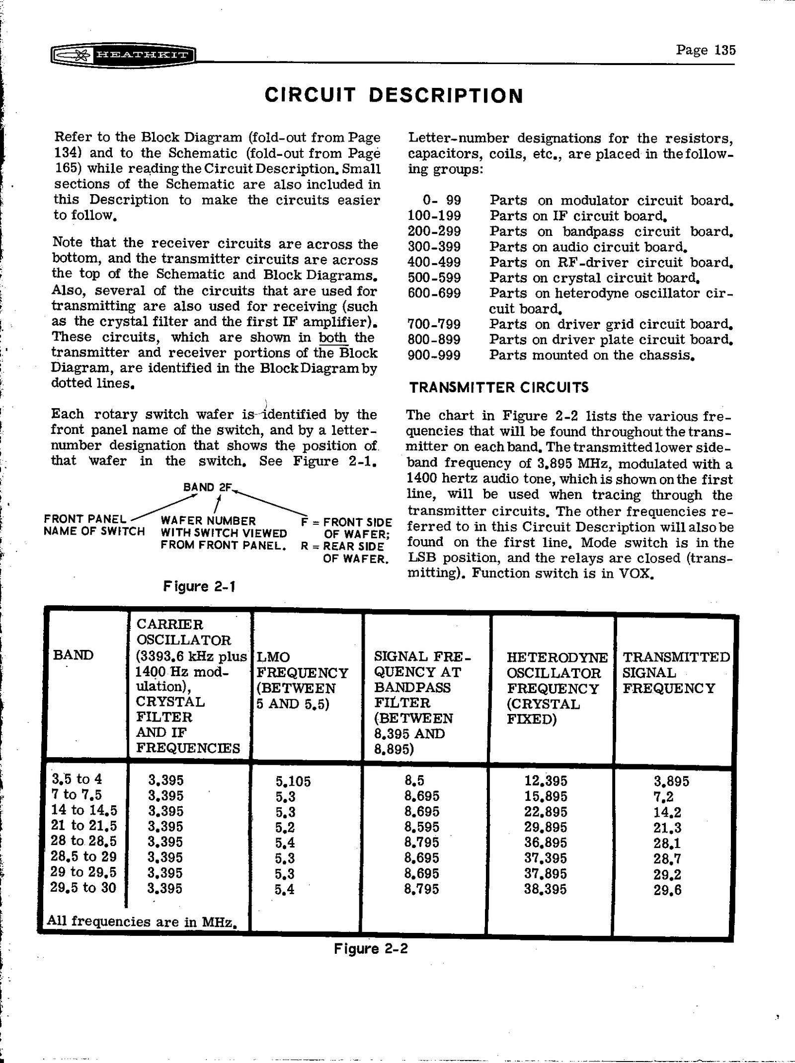
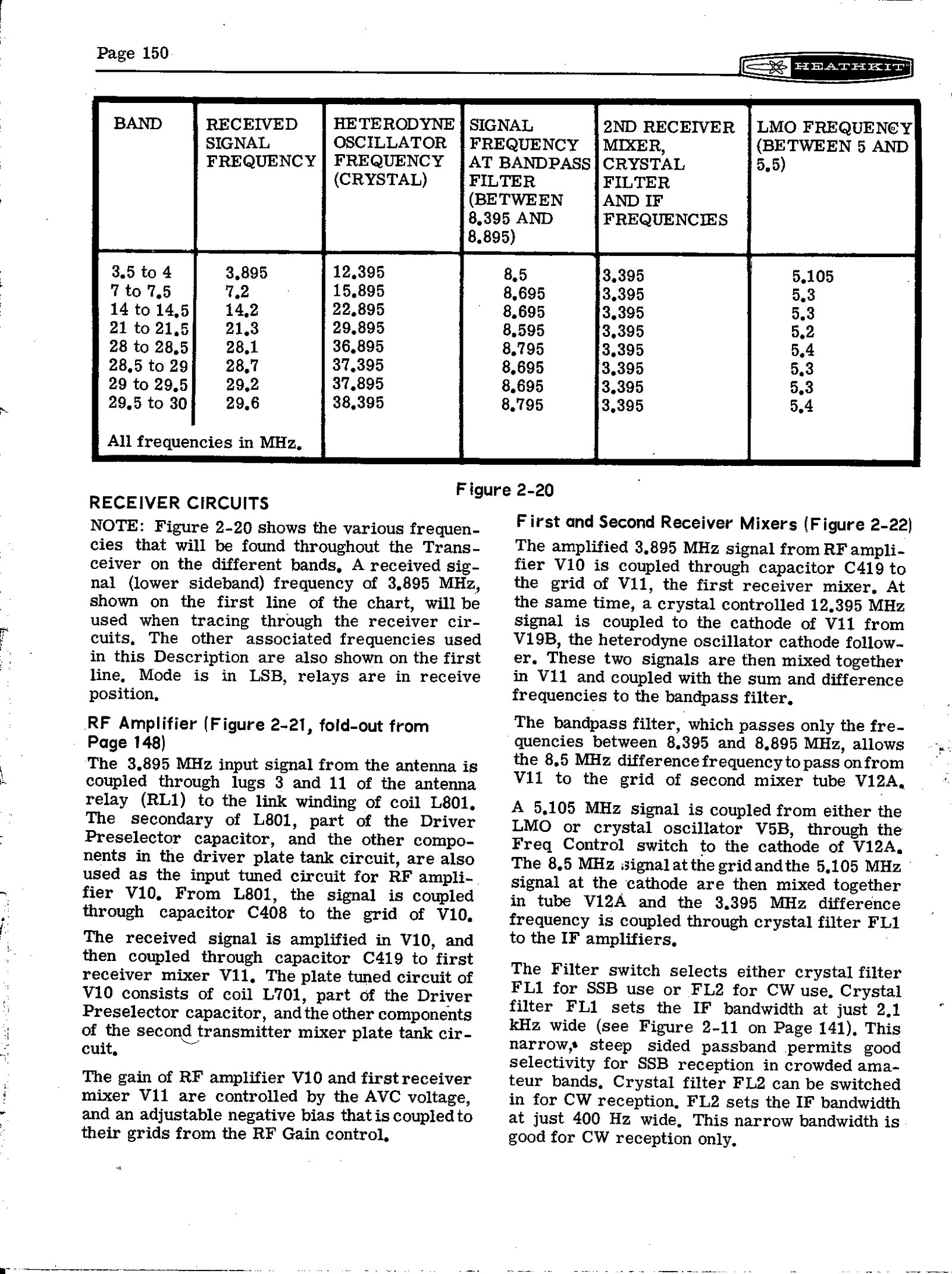
The arithmetic is the same as on every SB and HW transceiver. On 80 metres, a speech-band signal generated around the 3393.6 kHz lower-sideband carrier passes through the crystal filter as an upper sideband near 3.395 MHz. The first transmitter mixer adds the LMO; at an LMO setting of 5.105 MHz the sum is 8.5 MHz, inside the 8.395–8.895 MHz window of bandpass transformer T202. The second transmitter mixer subtracts that from the 12.395 MHz heterodyne crystal, leaving 3.895 MHz. Because the second mixer takes a difference, the sideband inverts and the upper sideband at the filter goes out as lower sideband.
The same subtraction explains why the LMO tunes “backwards”. Heath’s LMOs run from 5.5 MHz at the low end of each band down to 5.0 MHz at the top. At 5.5 MHz the first IF is 8.895 MHz and the output is 12.395 − 8.895 = 3.5 MHz; at 5.0 MHz the output is 4.0 MHz. Every band is exactly 500 kHz wide for the same reason, which is why 10 metres takes four band-switch positions.
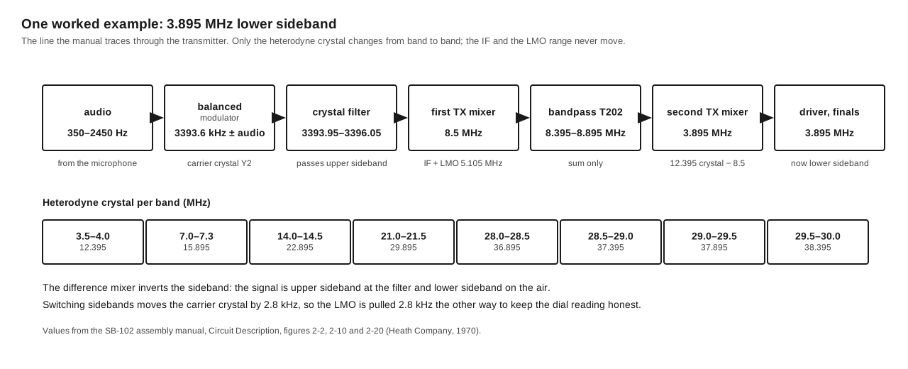
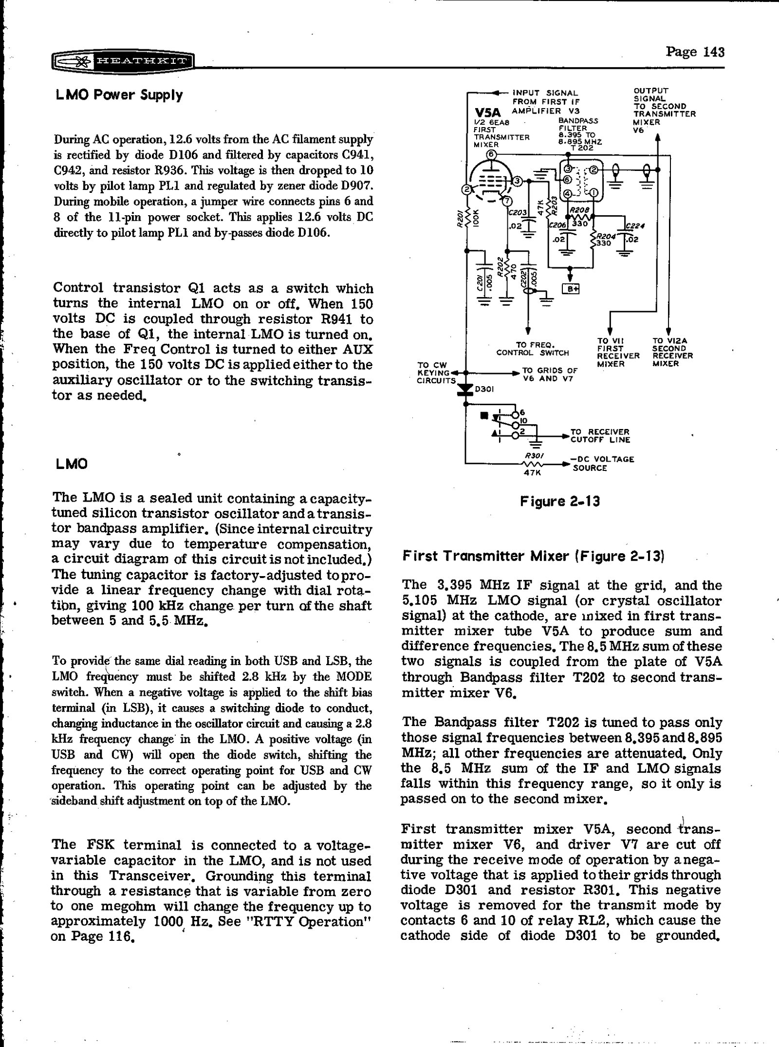
One crystal filter serves both sidebands because the carrier moves rather than the filter. Switching from lower to upper sideband moves the carrier from 3393.6 to 3396.4 kHz, which puts the passband on the other side of the carrier, and would shift the transmitted frequency by 2.8 kHz if nothing else changed. The MODE switch therefore also pulls the LMO by 2.8 kHz in the opposite direction, so the dial reads the same on either sideband. In the HW-101 a diode switches a capacitor across the FET VFO’s tuned circuit; in the SB-102 the same job is done inside the sealed LMO, as described below.
2.2 The LMO
2.2.1 What the manual says
The manual is unusually reticent about the one sub-assembly the builder never assembles. It describes the LMO as “a sealed unit containing a capacity-tuned silicon transistor oscillator and a transistor bandpass amplifier”, and explains that “since internal circuitry may vary due to temperature compensation, a circuit diagram of this circuit is not included.” Its tuning capacitor “is factory-adjusted to provide a linear frequency change with dial rotation, giving 100 kHz change per turn of the shaft between 5 and 5.5 MHz.” The LMO has four connections that matter to the rest of the set:
- A +10 V supply, from the LMO power supply described below.
- The shift-bias terminal. A negative voltage from the MODE switch in LSB makes a switching diode conduct, changing the inductance of the oscillator circuit and moving the frequency by 2.8 kHz. A positive voltage in USB and CW opens the diode. The operating point is trimmed by the sideband-shift adjustment on top of the LMO, which the alignment instructions call the LSB ADJUST screw.
- The FSK terminal. This connects to a voltage-variable capacitor inside the LMO. The terminal is unused in normal operation; grounding it through a resistance variable from zero to one megohm moves the frequency by up to about 1000 Hz, which is the basis of the manual’s short section on RTTY.
- The RF output, by coaxial cable to the FREQ CONTROL switch.
The manual’s troubleshooting chart ends every LMO fault in the same place: if the unit itself is defective, “return the complete LMO to the Heath Company”. Opening it voids the warranty. Its replacement price in the manual’s parts list is $94.00, about a quarter of the price of the whole kit. The 2.1 kHz crystal filter, a few lines below it, is $35.50, and a 6146 is $4.35.
2.2.2 What is inside
A redrawn schematic of the solid-state LMO circulates among restorers. It was drawn in January 2004 by J. Flanagan (WB5KYE) from an original lent by Harold Johnson (W4ZCB), and its title block describes it as the LMO “as originally drawn by TRW on 9-24-1969”, with several values marked as unreadable or unspecified (Internet Archive). It shows four transistors:
- Q1, a 2N706, the oscillator, running from a 1N755A zener-regulated rail and tuned by transformer T1, two trimmers, and fixed capacitors including one marked “Temp Comp”.
- CR3, an SM710 switching diode, fed from an “LSB/USB” terminal marked for +10 V or −100 V, which switches inductor L1 in and out of the tank. This is the 2.8 kHz sideband shift.
- CR2, a 1N3182, coupled into the tank through a small capacitor and biased from the FSK and back-bias terminals. This is the voltage-variable capacitor for frequency-shift keying.
- Q2 and Q3 (2N706) and Q4 (an RCA 40080), the amplifier chain that buffers the oscillator. Tuned coils L2, L3 and L4 at Q4’s output form the “bandpass amplifier” the manual mentions.
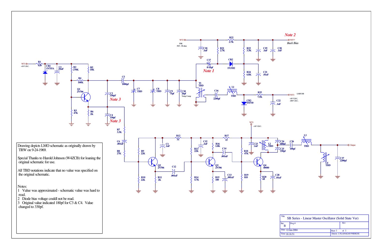
Who built the LMO is not settled. The restoration manual used throughout this dive states that the tube LMOs of the SB-100 and SB-101 were built by TRW but that “TRW did not build the LMO for the SB-102”, and that the SB-102’s LMO is the same one used in the solid-state SB-303 receiver and its shortwave twin, the SB-313 (W5RKL/WB8JKR restoration manual, section a.3.6). The redrawn schematic’s title block says the original drawing was TRW’s, dated September 1969, a few months before the SB-102 appeared. The two statements cannot both be right as written. The dive records both and does not decide between them.
2.2.3 The line of LMOs
The restoration manual tabulates Heath’s LMOs by part number, and the table is the simplest way to see where the SB-102’s sits.
Table 1 — The line of LMOs
| Part | Active device | Used in |
|---|---|---|
| 110-13 | 6AU6 | SB-300, SB-400 |
| 110-28 | 6BZ6 | SB-110 |
| 110-32 | 6BZ6 | SB-100, SB-401 |
| 110-40 | 6CB6 | SB-101, SB-301 |
| 110-48 | transistors | SB-102 |
The tube LMOs share a mechanism described in the restoration manual: a variable capacitor geared so that about five turns of the drive shaft turn it once, with a stack of six stop washers on the drive shaft limiting the travel, each picking up the next as it turns, until the last one meets a pin on the frame. When the grease on those washers hardens, the LMO stops short of its five turns, a fault the restoration volume returns to. The SB-102’s LMO also has five turns of travel from end to end; whether its stop mechanism is the same inside has not been confirmed.
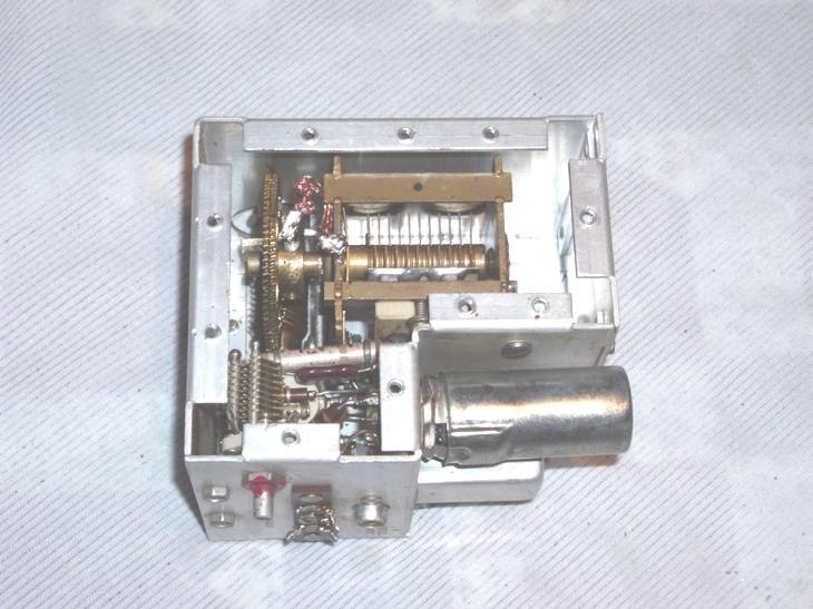
2.2.4 The LMO power supply
The tube LMOs took regulated 150 V from the transceiver’s B+ line. The SB-102’s needs 10 V, and gets it from a small power supply chassis that bolts to the top of the LMO. In AC operation, 12.6 V from the heater supply is rectified by a diode, filtered by capacitors C941 and C942 (500 µF each) and resistor R936, dropped to 10 V by a pilot lamp, PL1, used as a series resistor, and regulated by zener diode D907. In mobile operation a jumper between pins 6 and 8 of the 11-pin power socket applies 12.6 V DC to the pilot lamp directly and bypasses the rectifier. The initial test checks for exactly this: the lamp in the LMO supply “should glow dimly”.
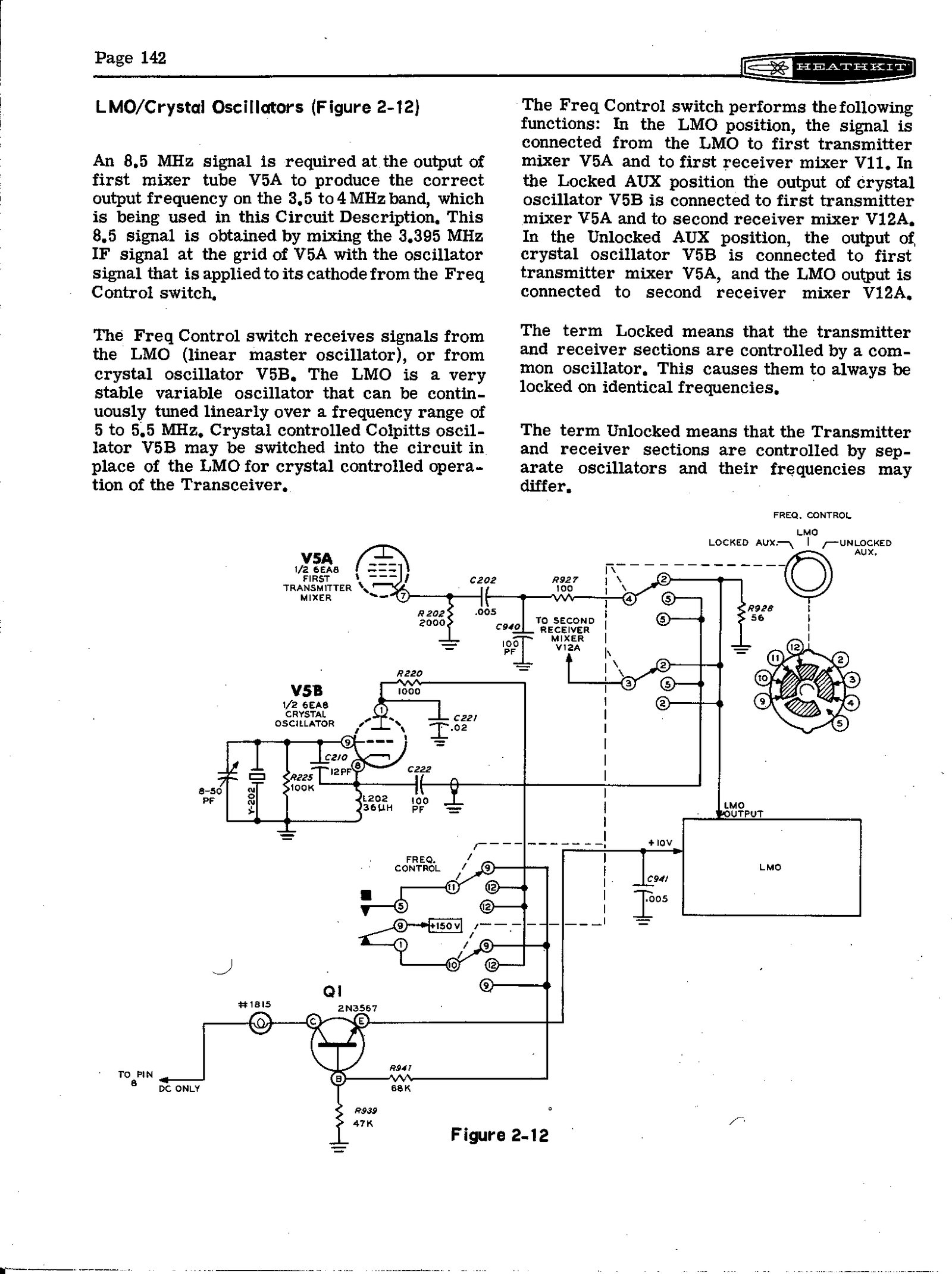
A 2N3567, Q1, acts as the switch that turns the internal LMO on. With the FREQ CONTROL switch in its LMO position, 150 V DC through resistor R941 at Q1’s base turns the LMO on. In either AUX position the 150 V goes instead to the auxiliary oscillator or to the switching transistor, as the mode requires.
2.3 FREQ CONTROL: locked and unlocked
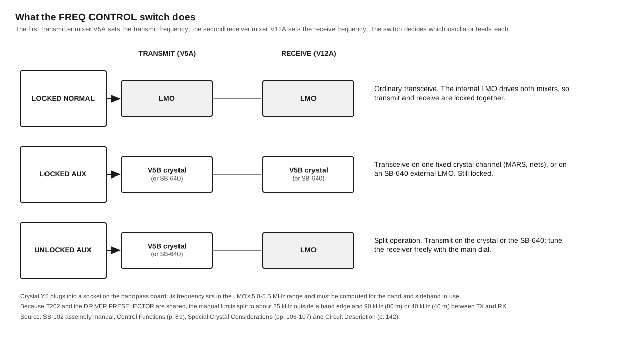
The first transmitter mixer, V5A, fixes the transmit frequency, and the second receiver mixer, V12A, fixes the receive frequency. The FREQ CONTROL switch decides which oscillator reaches each:
- LOCKED NORMAL. The LMO feeds both V5A and V12A. This is ordinary transceive operation.
- LOCKED AUX. Crystal oscillator V5B feeds both. The set transceives on one crystal-controlled frequency, for MARS or net work.
- UNLOCKED AUX. V5B feeds V5A and the LMO feeds V12A. The set transmits on the crystal and receives wherever the main dial is set.
With an SB-640 external LMO connected, the “AUX” signal comes from the SB-640 instead of V5B. That gives the combinations Heath advertised: transceive on either LMO, receive on the SB-102 and transmit on the SB-640, or transceive on either of the SB-640’s own two crystal frequencies. The manual adds a limit that applies to every split: because bandpass filter T202 is steep-sided and the DRIVER PRESELECTOR tunes the same circuits for transmit and receive, crystal operation is limited to about 25 kHz outside each band, and the split between transmit and receive to “about 90 kHz at 3.5 MHz, 40 kHz at 7 MHz, etc.”
2.4 The transmitter
The transmit chain is the one the SB-100 established and the HW-101 later copied, and the HW-101 dive describes it stage by stage. In outline:
- Speech amplifier and cathode follower, V1 (6EA8). V1A amplifies the microphone and feeds both the VOX circuit and the MIC LEVEL control; V1B drives the balanced modulator at low impedance and is biased off in TUNE and CW.
- Balanced modulator, CR1–CR4. A four-diode ring, nulled by the CARRIER NULL control and capacitor. In CW and TUNE the MODE switch grounds one side of the ring to unbalance it and produce a carrier.
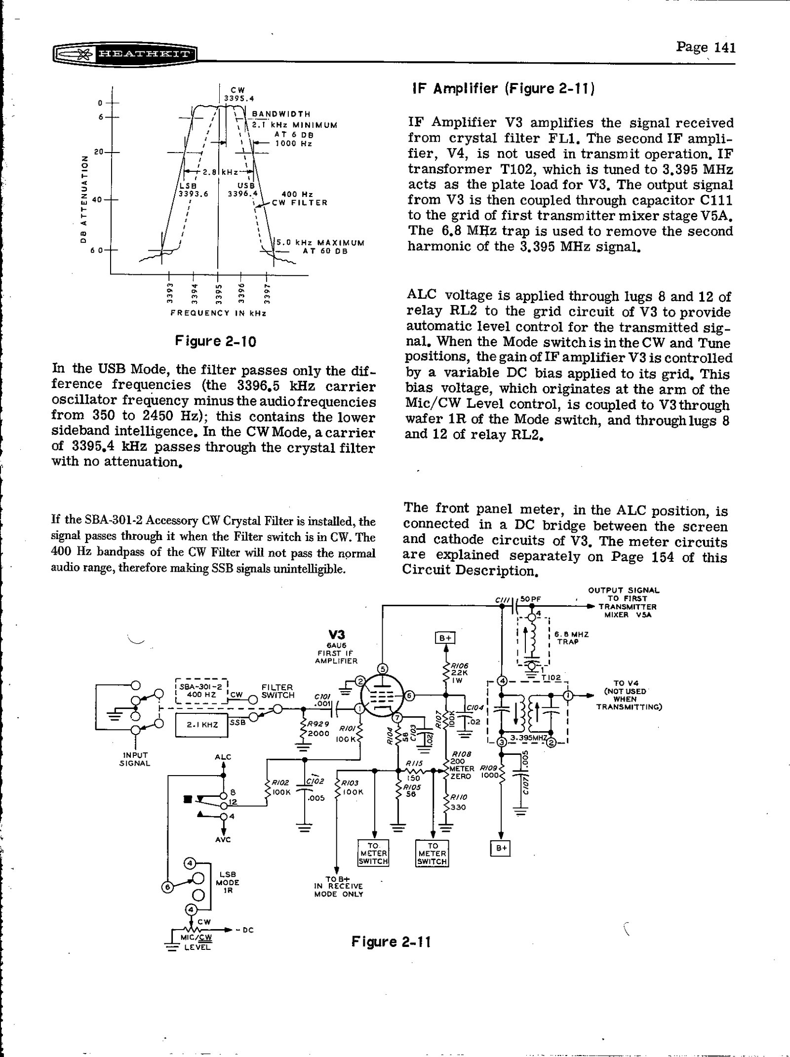
- Isolation amplifier, V2 (6AU6). Buffers the ring from the crystal filter. ALC, or the CW level bias, acts on its grid.
- Crystal filter FL1. Centre 3395 kHz, 2.1 kHz wide at the 6 dB points (3393.95 to 3396.05 kHz). With the modulator’s own balance, Heath claimed at least 50 dB of carrier attenuation at this point.
- First IF amplifier, V3 (6AU6). The one stage that amplifies at 3.395 MHz in both directions. A sealed 6.8 MHz trap removes the IF’s second harmonic before the first mixer.
- First transmitter mixer, V5A (6EA8), and bandpass filter T202. IF on the grid and LMO or crystal on the cathode; the 8.395–8.895 MHz sum goes on.
- Second transmitter mixer, V6 (6CB6). Heterodyne crystal on the cathode; the operating frequency is taken from a plate tank tuned by the DRIVER PRESELECTOR.
- Driver, V7 (6CL6). Neutralised by a “neutralizing wire” run from the preselector into the plate area, whose position is set during alignment.
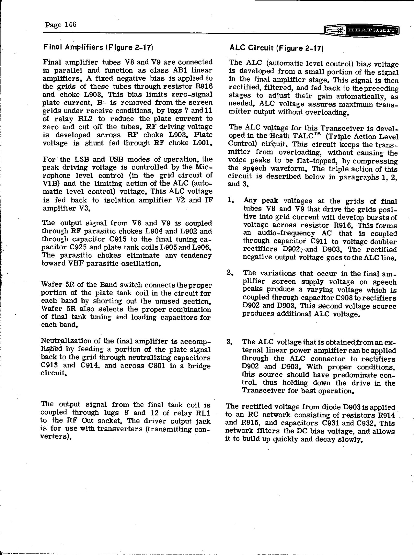
- Finals, V8 and V9 (two 6146). Class AB1 in parallel, with fixed negative bias, parasitic chokes in the plate leads, a pi network tuned and loaded from the front panel, and neutralisation by C913 and C914.
- TALC. Heath’s Triple Action Level Control rectifies three sources — final grid current across R916, screen-supply variation coupled through C908, and ALC from an external linear — into one negative line with a fast attack and slow decay, fed back to V2 and V3.
2.4.1 The Miller-effect switch
The DRIVER PRESELECTOR is two ganged variable capacitors. One section tunes the second transmitter mixer’s plate tank, which becomes the RF amplifier’s plate tank on receive; the other tunes the driver’s plate tank, which becomes the receiver’s input circuit. Tube capacitance differs between the two modes because of Miller effect, so on early SB transceivers the control peaked at different settings in receive and transmit. The SB-102 corrects this with diode D909. A negative voltage from the BIAS ADJUST control always sits on D909’s anode. On receive, a larger positive voltage from V11’s screen circuit, through R955, makes the diode conduct, and it grounds capacitor C955, putting it in parallel with the preselector section C421B. On transmit, relay RL2 removes the positive voltage, the diode opens, and C955 drops out.
This is the circuit that the SBM-102-1 modification kit added to the SB-100, the SB-101 and early SB-102s. Eckweiler gives the serial-number break as 5446 and recommends the kit to every owner of an earlier set “to improve receiver sensitivity and transmitter drive” (Heathkit of the Month #30). The 595-1058-06 manual describes the circuit as standard, so that edition, at least, belongs to the later production.
2.5 The receiver
Received signals travel the same chain backwards. The antenna relay feeds a link winding on L801, the driver’s plate coil, so the DRIVER PRESELECTOR tunes the receiver front end and the transmitter driver with the same capacitors.
- RF amplifier, V10 (6HS6). This is the SB-102’s receiver change. The SB-100 and SB-101 used a 6AU6 here; the SB-102 uses a 6HS6, a higher-gain pentode, for the “hotter receiver” of the catalogue copy.
- First receiver mixer, V11 (6AU6). Heterodyne crystal on the cathode, output into bandpass filter T202. The manual’s specification page and its figure 2-22 both show a 6AU6 here. The restoration manual confirms that the SB-102 uses the 6HS6 “ONLY in the receiver’s RF amplifier”, while the later HW-101 uses 6HS6s in both positions.
- Second receiver mixer, V12A (6EA8). LMO or crystal on the cathode, 3.395 MHz out to the crystal filter.
- Crystal filters FL1 and FL2. The FILTER switch selects the 2.1 kHz SSB filter or, if fitted, the SBA-301-2 400 Hz CW filter. The SB-101 introduced this front-panel selection; the SB-100 did not have it.
- IF amplifiers, V3 and V4 (6AU6), and AVC. V13A and V13B, in a 6BN8, rectify part of the IF into a negative AVC voltage across two capacitors: C124 charges quickly to catch peaks and C110 slowly to follow the average. The result is the fast-attack, slow-release characteristic SSB needs. A two-diode gate lets either the AVC or the RF GAIN control’s bias set the gain of V10, V11, V3 and V4.
- Product detector, V13C, and audio, V14 (6GW8). The carrier oscillator beats the IF down to audio. The power stage delivers 2 W to an 8 Ω speaker, with a separate high-impedance headphone output and, on the SB-102, a headphone volume control.
2.6 Changing over, CW and the calibrator
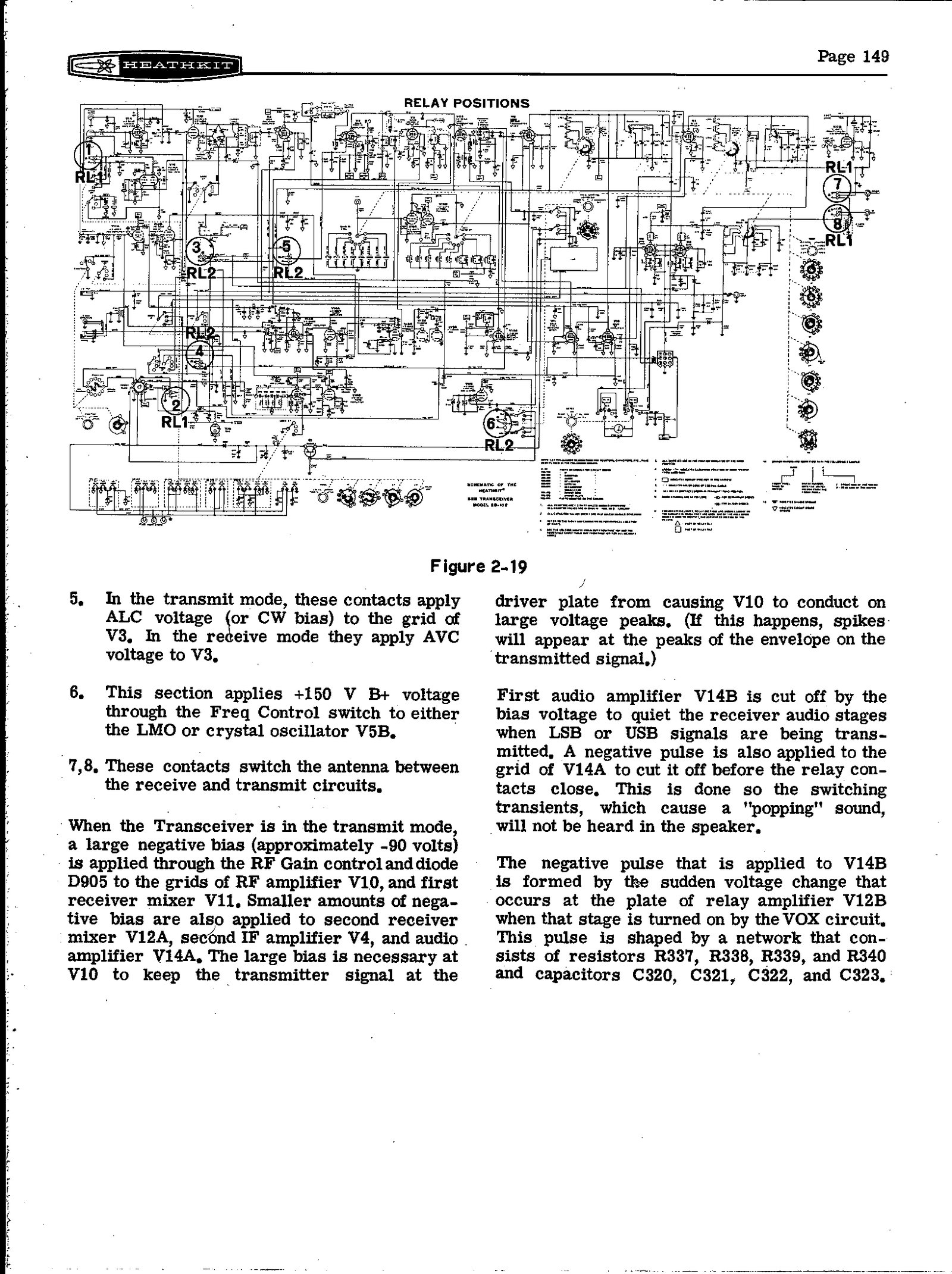
Two relays do the switching. RL1 changes the antenna over. RL2 moves B+ between the screens of the transmit and receive tubes, swaps ALC and AVC at V3’s grid, grounds whichever cut-off bias is not wanted, and applies +150 V through the FREQ CONTROL switch to the LMO or to V5B. A spare set of contacts, rated 3 A at 30 V DC or 120 V AC, is brought out to the power plug for keying a linear amplifier. Relay amplifier V12B drives both relays. Push-to-talk, the VOX circuit (V17A with rectifier D201), or the CW tone switches it on, and anti-trip rectifiers D1 and D2 cancel the VOX voltage that the speaker would otherwise produce.
On transmit the receiver is silenced hard. About −90 V is applied through the RF GAIN control and D905 to the grids of V10 and V11, and smaller amounts to V12A, V4 and the audio. A shaped negative pulse from V12B’s plate cuts off the first audio stage before the relay contacts close, so the switching click is not heard.
CW works by a set of small deceptions common to filter-type SSB rigs. In CW, the MODE switch cuts off the speech cathode follower, grounds the VOX sensitivity control, connects Y3 to the carrier oscillator, unbalances the modulator, biases off the transmit mixers and driver, and starts the tone oscillator V15A, a phase-shift oscillator at about 1000 Hz. Closing the key removes the mixers’ cut-off bias and sends the tone into the VOX circuit, which keys the relays; the same tone feeds the speaker as sidetone. On receive, V16A and Y1 act as the beat oscillator, placed so that a station on the transmitting frequency is heard as a 1000 Hz note. The operating section of the manual puts it in practical terms: the transmitted CW signal is 1000 Hz above the dial reading, and because the receiver is effectively in USB, an SB-102 on CW and another station on USB can work each other without retuning.
The 100 kHz crystal calibrator, V17B, is a Pierce oscillator switched on by the CAL position of the FUNCTION switch. It is coupled through C218 and diode CR201 to the antenna input, and trimmer C220 sets it exactly on frequency against WWV.
2.7 Metering
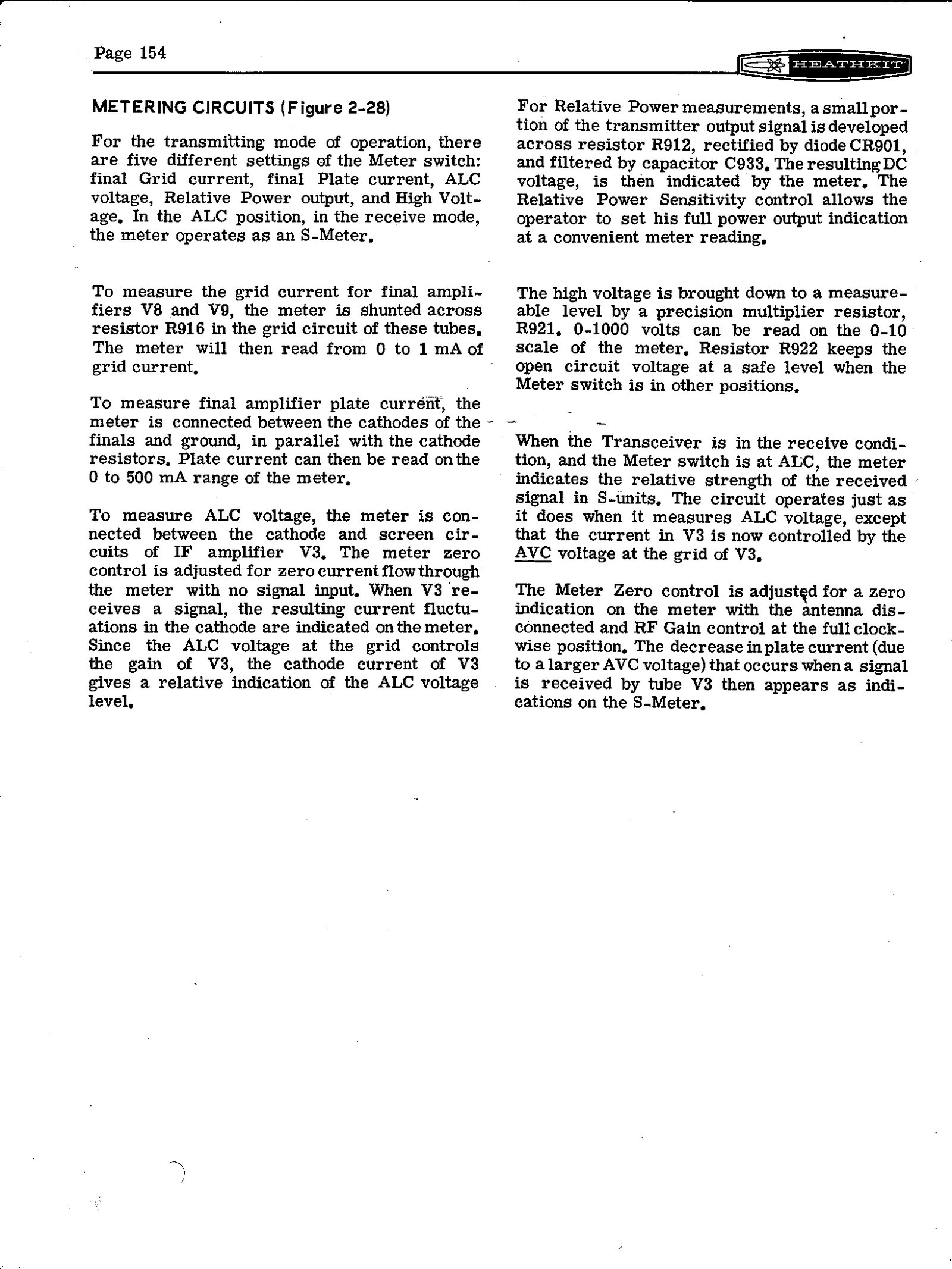
The single meter reads five things on transmit, one more than the HW-101’s four:
- GRID. The meter is shunted across R916 in the finals’ grid circuit and reads 0 to 1 mA of grid current.
- PLATE. The meter sits between the finals’ cathodes and ground and reads 0 to 500 mA.
- ALC. The meter is in a DC bridge between V3’s screen and cathode. On receive the same position is the S-meter, reading from 0 up to 60 dB over S9.
- REL PWR. A sample of the output across R912 is rectified by CR901 and filtered by C933. An internal RELATIVE POWER sensitivity control sets full scale.
- HV. The high-voltage line is read through precision multiplier R921 on the 0–10 scale, as 0 to 1000 V. R922 keeps the open-circuit voltage safe in the other switch positions.
2.8 Reading the chassis
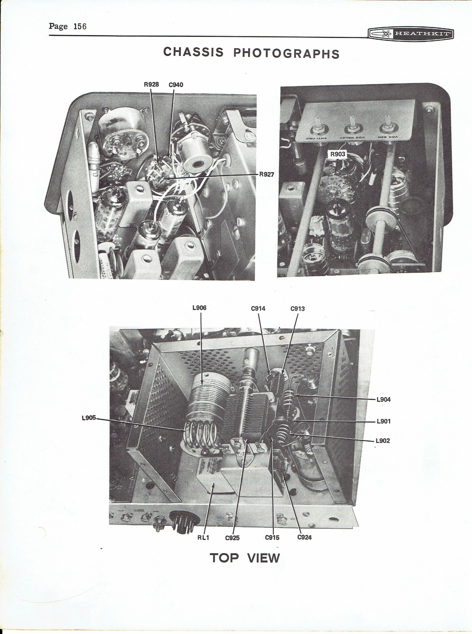
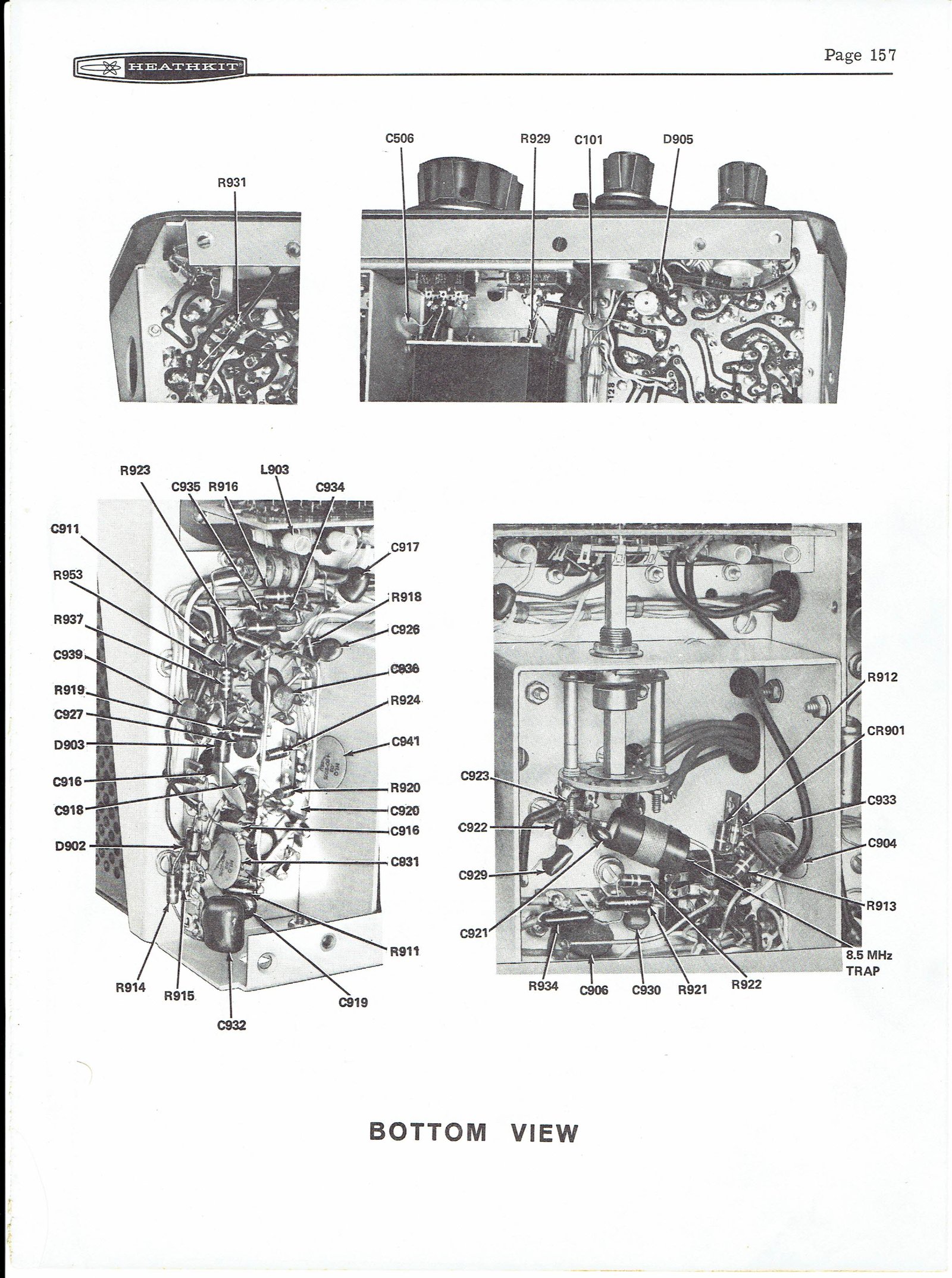
Heath’s designator scheme makes the schematic navigable. The hundreds digit of a designator names its board: 0–99 modulator, 100–199 IF, 200–299 bandpass, 300–399 audio, 400–499 RF driver, 500–599 crystal, 600–699 heterodyne oscillator, 700–799 driver grid, 800–899 driver plate, and 900–999 the chassis. Rotary switch wafers are named by the panel control, a wafer number and F or R for the front or rear face. The manual’s chassis photographs are labelled with the same designators, so a part named in the troubleshooting chart can be found in the metal.
2.9 What the SB-102 bought
The SB-102’s circuit is not radically different from the SB-101’s; the catalogue called it “the world’s best rig (the SB-101)… now even better”, and that is a fair summary. What changed is where the heat and drift came from. A tube oscillator in a closed box warms slowly and drifts as it does, which is why the earlier sets needed 20 minutes; a transistor oscillator dissipates almost nothing, so the SB-102 settled in 10. The 6HS6 front end and the Miller-effect switch improved the receiver and made the preselector track. What the SB-102 did not change was the set’s architecture: a 1960s crystal-filter transceiver with a mechanical dial, no receiver incremental tuning and an outboard power supply. Heath’s next step, the SB-104, abandoned all three.
Sources
- Heathkit Assembly Manual, SSB Transceiver Model SB-102, 595-1058-06 (Heath Company, 1970), Circuit Description pp. 135–155, Specifications pp. 131–134, Chassis Photographs pp. 156–157. W5RKL · Internet Archive (pp. 88 onward)
- Flanagan, J. (WB5KYE). “SB Series – Linear Master Oscillator (Solid State Ver),” redrawn schematic, 12 January 2004. Internet Archive
- Kembel, Robert W. (W5RKL), Mark (WB8JKR) and contributors. Heathkit HW-101 and SB-10x Restoration and Troubleshooting, revised 17 December 2021: sections a.3 (SB vs HW series) and af (Heathkit Linear Master Oscillators). PDF
- Eckweiler, Bob (AF6C). “Heathkit of the Month #30: The Amateur Radio SB-Line Overview,” 2011 — for the SBM-102-1 kit and the LMO. PDF
- Heathkit catalogue 800/03 (summer 1970), p. 54, for Heath’s own statement of the changes from the SB-101. World Radio History
- The shared transmitter and receiver stages: HW-101 dive, How It Works.
Comments (0)