HW-101 Transceiver · Volume 2
How It Works
The HW-101 is a filter-type single-sideband transceiver in the classical form: generate the sideband once, at a fixed low frequency where a crystal filter can be cheap and sharp, then heterodyne it up to the operating frequency in two steps, and run the whole chain backwards to receive. Nothing in it is novel. What is interesting is the economy with which Heath arranged the sharing — one crystal filter, one first IF amplifier, one VFO, one heterodyne crystal and one set of driver tank coils do duty in both directions — because every stage that serves twice is a stage the customer does not pay for twice.
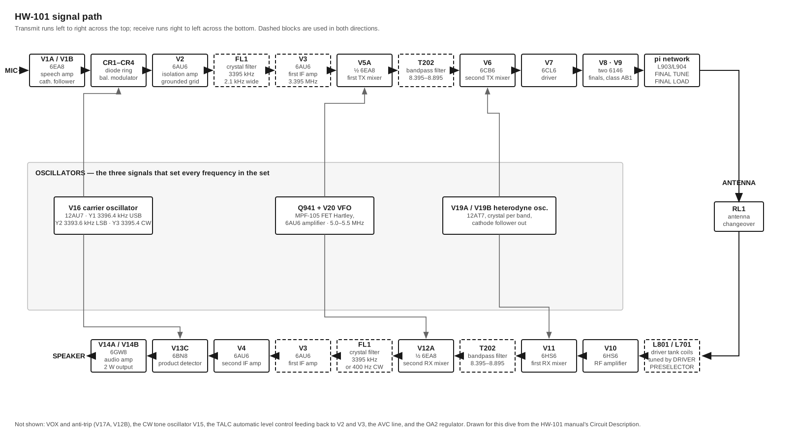
2.1 The frequency scheme
Three oscillators set every frequency in the set.
The carrier oscillator, V16 (a 12AU7), is two Colpitts crystal oscillators sharing one envelope. One half runs crystal Y1 at 3396.4 kHz for upper sideband; the other runs Y2 at 3393.6 kHz for lower sideband and Y3 at 3395.4 kHz for CW. The mode switch chooses which half gets B+ and which crystal reaches the grid.
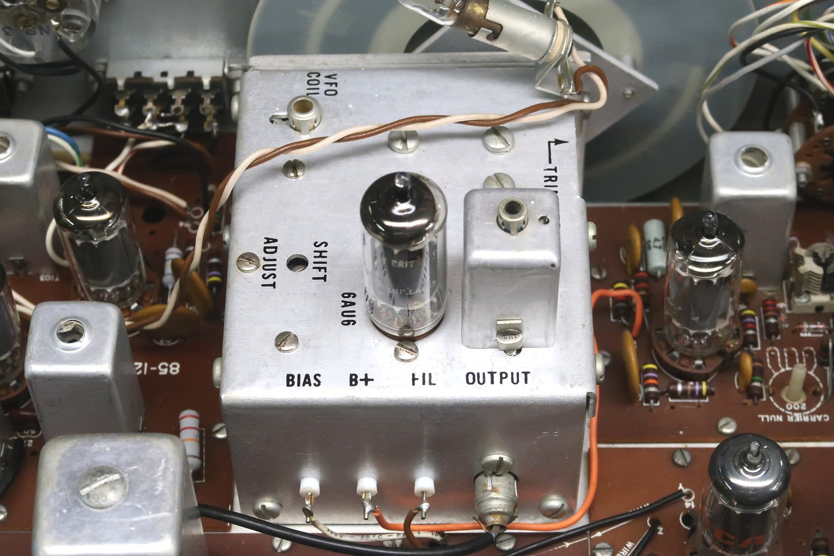
The VFO covers 5.0 to 5.5 MHz on every band. It is the one stage in the receiver-transmitter chain that is not a tube: an MPF-105 field-effect transistor in a Hartley circuit, with part of coil L941 and the main tuning capacitor C950A setting the frequency, the remainder of the coil providing feedback, and a string of fixed temperature-compensating capacitors holding it steady. A 6AU6, V20, amplifies the output and couples it through T941 to the mixers. The transistor in V20’s cathode is a 2N3393 used backwards — base-emitter junction only — as a cheap zener diode.
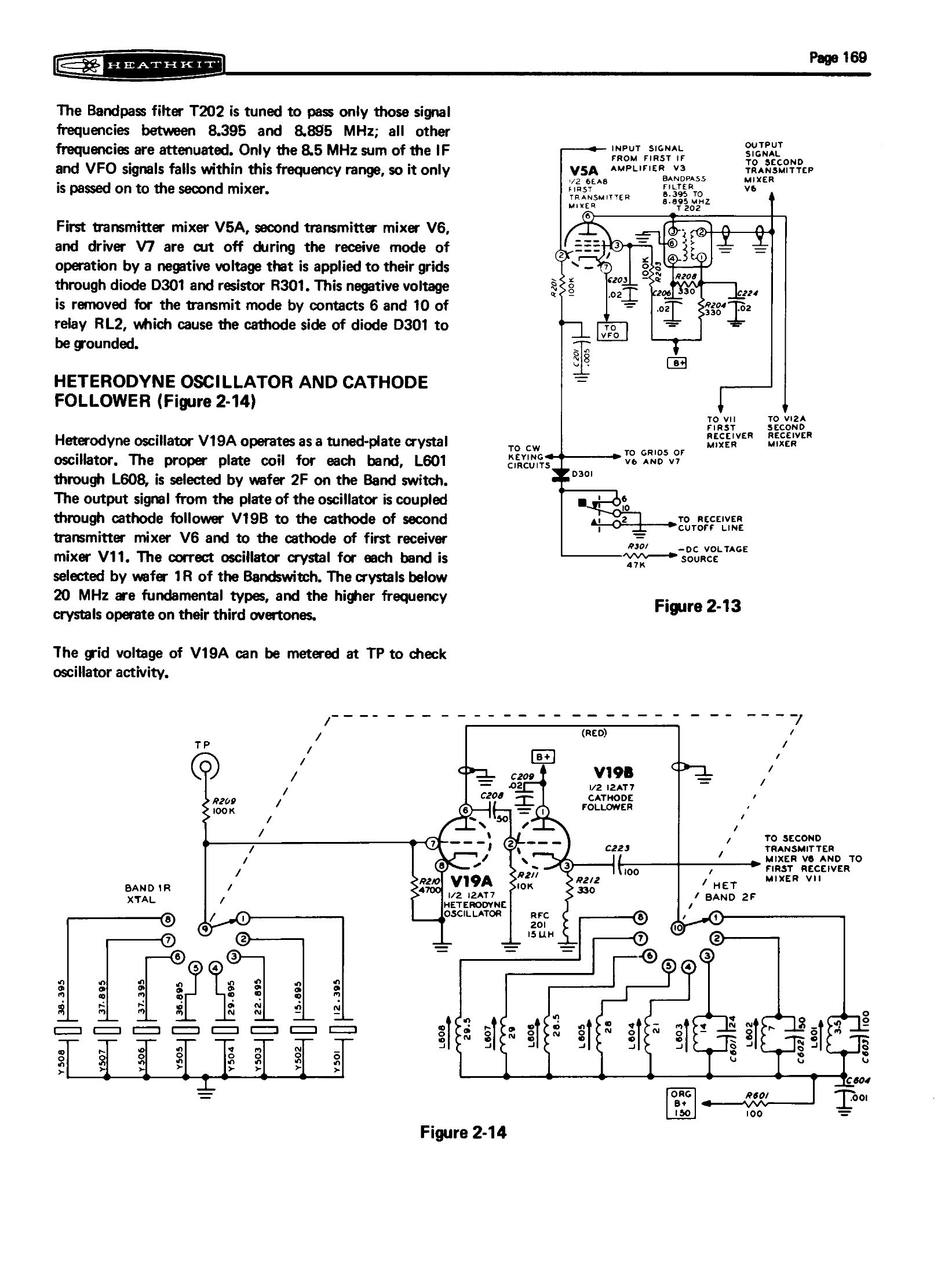
The heterodyne oscillator, V19A (half a 12AT7), is a tuned-plate crystal oscillator with one crystal and one plate coil per band, selected by two wafers of the band switch. Crystals below 20 MHz are fundamental types; the higher ones run on their third overtone. V19B is a cathode follower that feeds the oscillator’s output to both the second transmitter mixer and the first receiver mixer without letting either pull the oscillator.
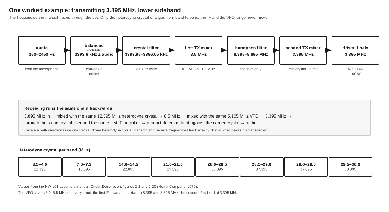
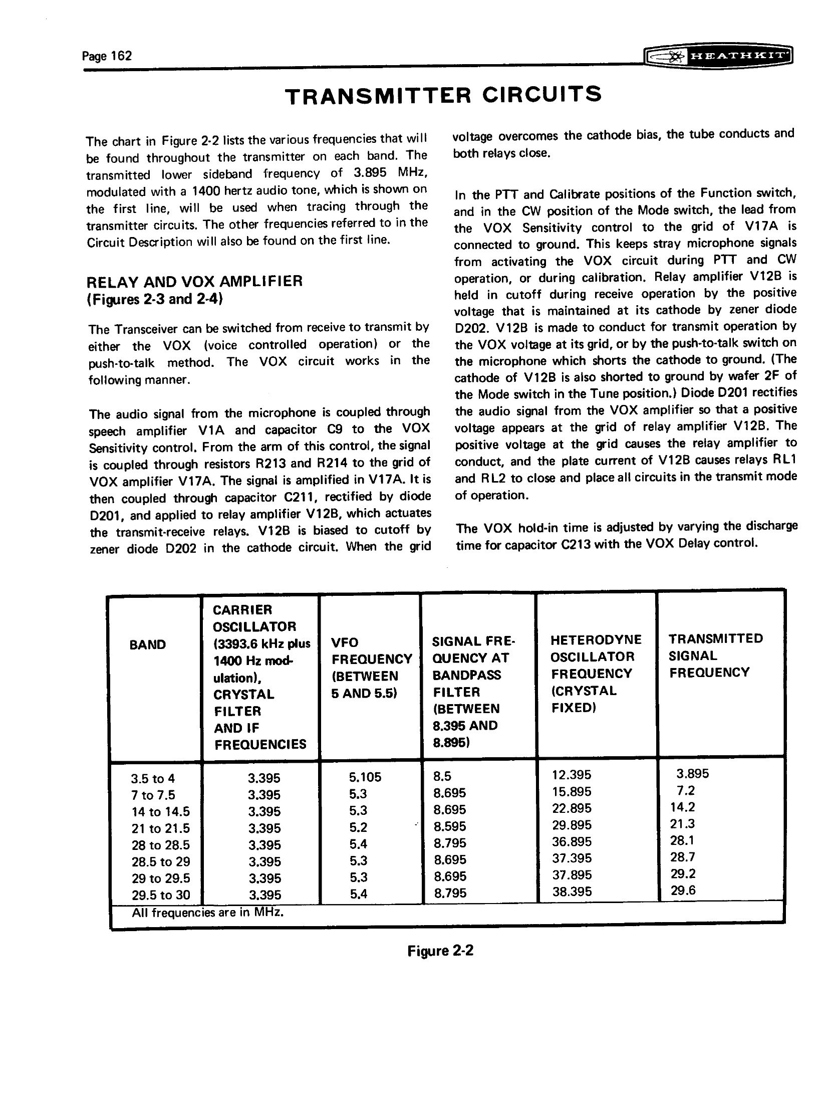
The arithmetic is worth following once, because it explains the whole architecture. On 80 metres, a 1400 Hz tone modulating the 3393.6 kHz carrier crystal produces sidebands either side of 3393.6 kHz. The crystal filter, centred on 3395 kHz and 2.1 kHz wide, passes only the sum frequencies — the upper sideband of that carrier, which carries the intelligence — and attenuates the carrier itself by a further 20 dB. Mixing that with the VFO at 5.105 MHz gives 8.5 MHz, which falls inside the 8.395–8.895 MHz window of the bandpass transformer T202; every other product is rejected. Mixing 8.5 MHz with the heterodyne crystal at 12.395 MHz gives the difference, 3.895 MHz, which is what goes out of the antenna — and because the second mixer takes a difference, the sidebands invert, so the signal that was an upper sideband at the filter is a lower sideband on the air.
That inversion is also how one crystal filter serves both sidebands. The filter never moves; the carrier crystal moves, from 3393.6 kHz to 3396.4 kHz, which shifts the passband from one side of the carrier to the other. Switching sidebands would shift the transmitted frequency by 2.8 kHz if nothing else changed, so the mode switch also changes the bias on diode CR941 in the VFO, switching capacitor C945 in or out and pulling the VFO by the offsetting amount. The internal control that trims this is the VFO SHIFTER, and it is the reason a well-aligned HW-101 reads the same dial frequency on both sidebands.
2.2 The transmitter
Speech amplifier and cathode follower (V1, a 6EA8). The microphone feeds V1A, whose plate signal goes two ways: to the VOX circuit, and through the MIC LEVEL section of the front-panel control to cathode follower V1B, which drives the balanced modulator at low impedance. In CW and TUNE, V1B is cut off by bias so that stray audio cannot reach the modulator.
Balanced modulator (CR1–CR4). Four germanium diodes in a ring, with the audio on one diagonal and the carrier on the other. With the carrier nulled by the CARRIER NULL control and its associated trimmer, and no audio applied, there is no output at all; audio unbalances the ring at an audio rate and the sum and difference frequencies — the two sidebands — appear across transformer T1. In CW and TUNE the mode switch grounds one side of the ring, deliberately unbalancing it so that a carrier does appear: that is how a filter-type SSB transmitter makes CW.
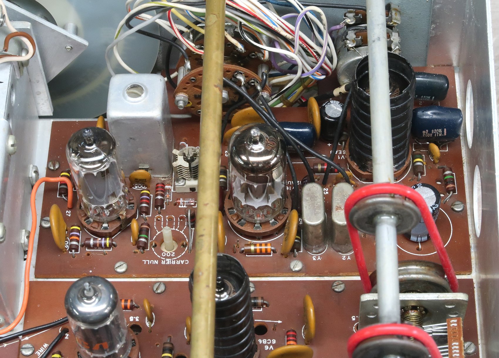
Isolation amplifier (V2, a 6AU6). A grounded-grid stage that isolates the diode ring from the crystal filter and matches impedances into it. It is also one of the two places where automatic level control acts: the ALC line, or a manually set bias from the MIC/CW LEVEL control in CW, sits on its grid and varies its gain.
Crystal filter FL1. Centre frequency 3395 kHz, usable bandwidth 2.1 kHz between the 6 dB points, which the manual gives precisely as 3393.95 to 3396.05 kHz. Between the balanced modulator’s own suppression and the filter’s further 20 dB of attenuation at the carrier frequency, Heath claimed at least 50 dB of carrier attenuation at this point and specified 45 dB at the antenna. If the optional SBA-301-2 filter is fitted, the front-panel filter switch puts its 400 Hz passband in circuit instead — too narrow to pass speech at all, which is why the manual warns that SSB signals become unintelligible with it selected.
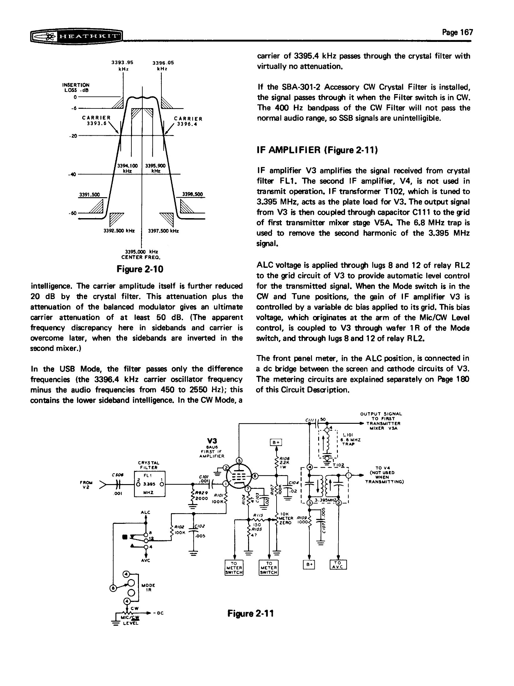
First IF amplifier (V3, a 6AU6). The only tube in the set that amplifies at 3.395 MHz in both directions. On transmit it drives the first transmitter mixer through a trap tuned to 6.8 MHz, which removes the second harmonic of the IF; on receive it feeds the second IF amplifier. Its cathode and screen circuits form the bridge that the front-panel meter reads as ALC on transmit and as S-units on receive — one meter circuit, two jobs, because the stage it watches is itself doing two jobs.
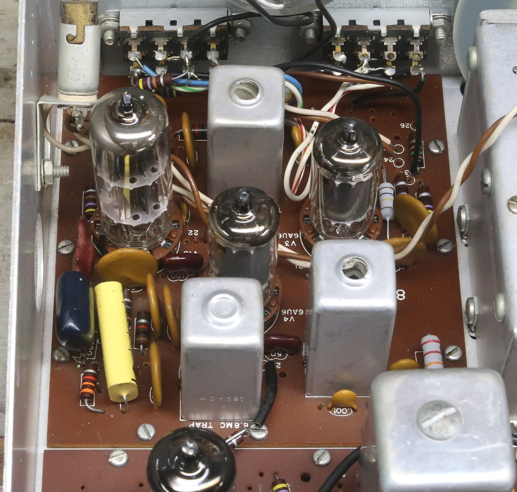
First transmitter mixer (V5A, half a 6EA8) and the bandpass filter. IF on the grid, VFO on the cathode, and the 8.5 MHz sum taken from the plate through the bandpass transformer T202. Because the VFO covers half a megahertz and the IF is fixed, this stage’s output is a variable intermediate frequency between 8.395 and 8.895 MHz — Heath’s specification sheets call it exactly that. The filter passes that half-megahertz window and rejects everything else, including the difference product.
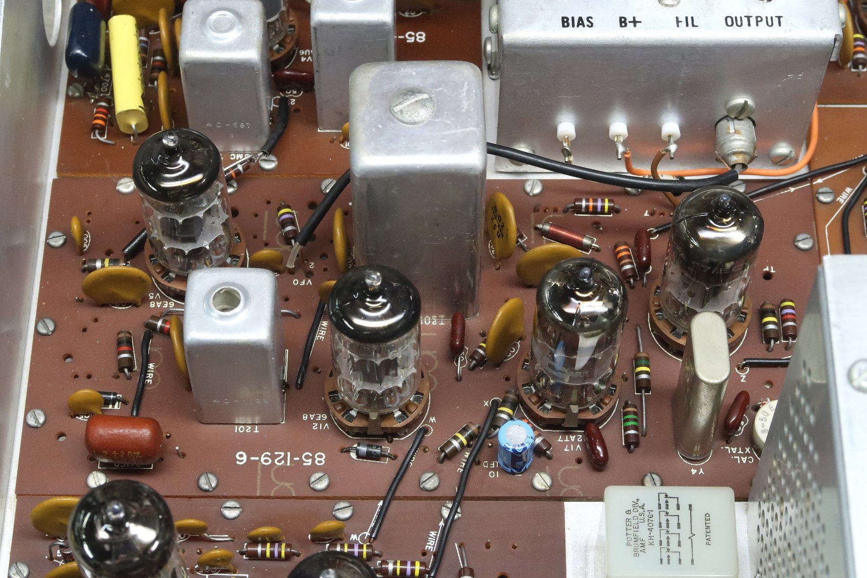
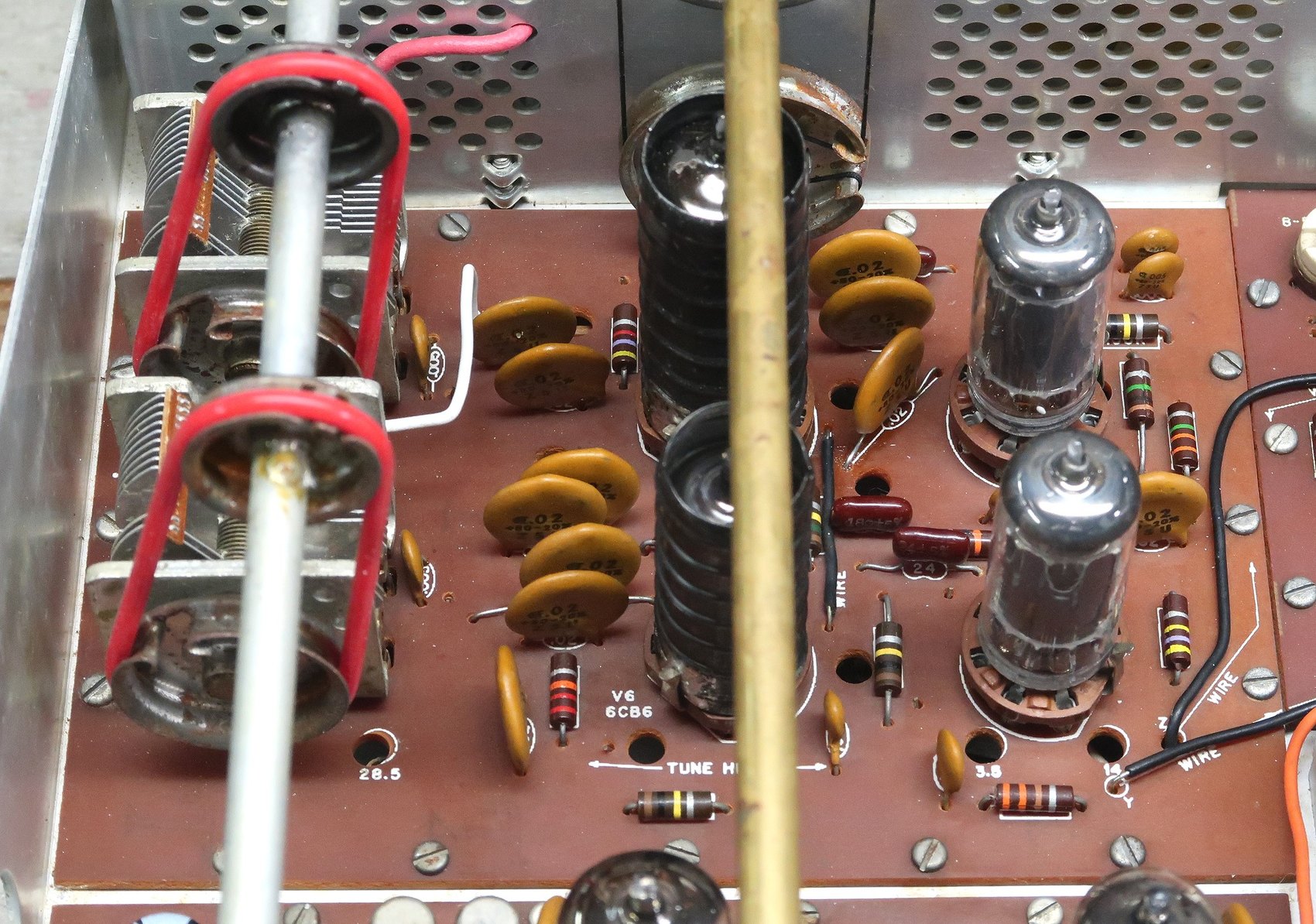
Second transmitter mixer (V6, a 6CB6). Bandpass signal on the grid, heterodyne crystal on the cathode, and the operating frequency taken from a plate tank tuned by the DRIVER PRESELECTOR. Coil L701 is across the tank on every band, with the band switch paralleling more inductance for the higher bands and switching additional capacitance for the lower ones.
Driver (V7, a 6CL6). Amplifies the operating-frequency signal to a level that will drive the finals, into another band-switched tank built around L801. V7 is neutralised, in one of the design’s more agricultural touches, by a length of insulated wire run from the driver preselector capacitor frame past the 6CL6’s plate — a gimmick capacitor whose value is set by how far the wire is pushed in.
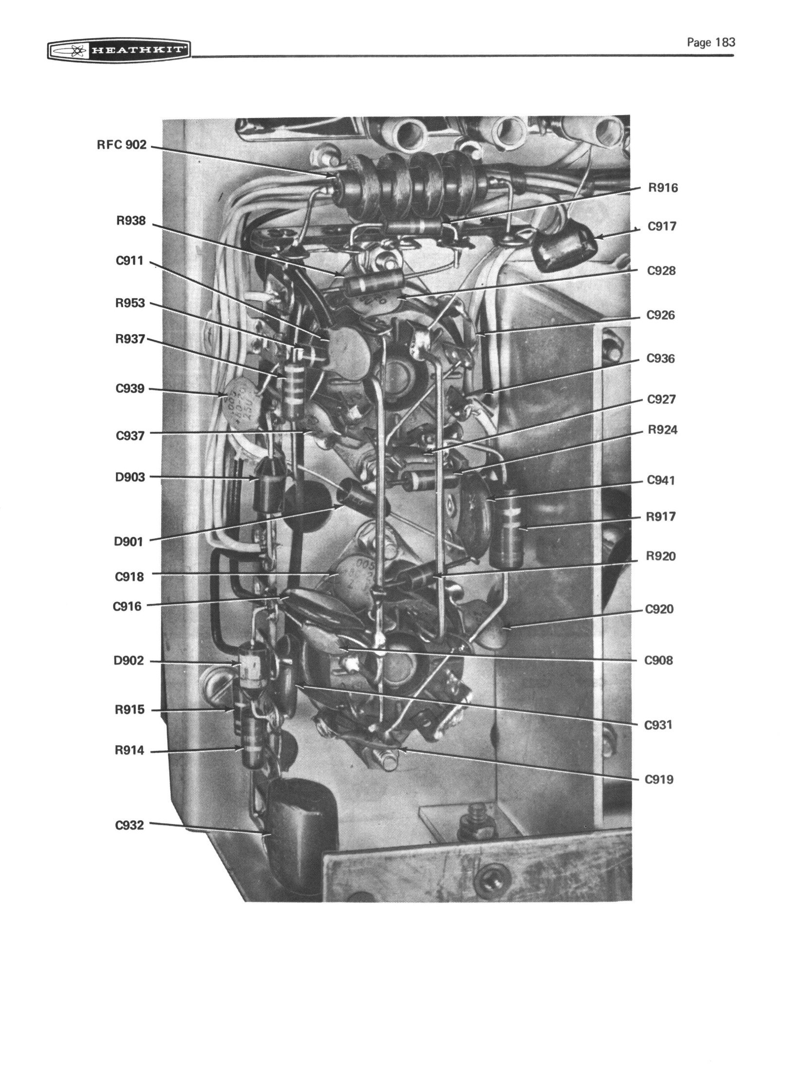
Final amplifiers (V8 and V9, two 6146 in parallel). Class AB1 linear amplifiers with fixed negative bias through R916 and RFC902, shunt-fed plate voltage through RFC901, and parasitic suppressors L901 and L902 in the plate leads. The output goes into a pi network — L903 and L904, FINAL tuning capacitor C925 and the loading capacitor — with band switch wafer 5R shorting out the unused part of the tank coil and selecting the right combination of tuning and loading capacitance. Neutralisation is by capacitors C913 and C914 feeding plate signal back to the grid circuit across C801 in a bridge.
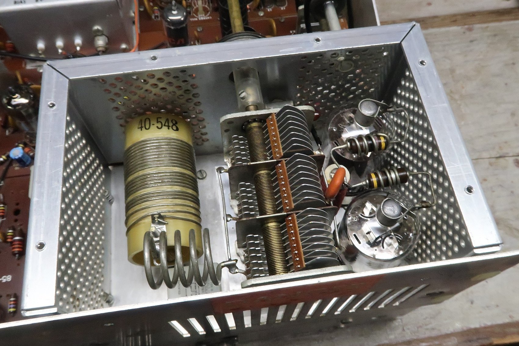
TALC. Heath’s trademarked Triple Action Level Control is the ALC system, and the “triple” is literal. Grid current in the finals develops pulses across R916; variations in the final screen supply on speech peaks are coupled through C908; and an external linear amplifier can inject its own ALC voltage at the rear socket. All three are rectified by the voltage-doubler pair D902 and D903 into one negative line, filtered so that it rises quickly and decays slowly, and fed back to the grids of the isolation amplifier V2 and the first IF amplifier V3. On CW no ALC is developed at all; the drive is set manually with the MIC/CW LEVEL control instead.
2.3 The receiver
Received signals travel the same chain in reverse, and the manual’s own frequency chart for the receiver is the transmit chart with the columns read the other way.
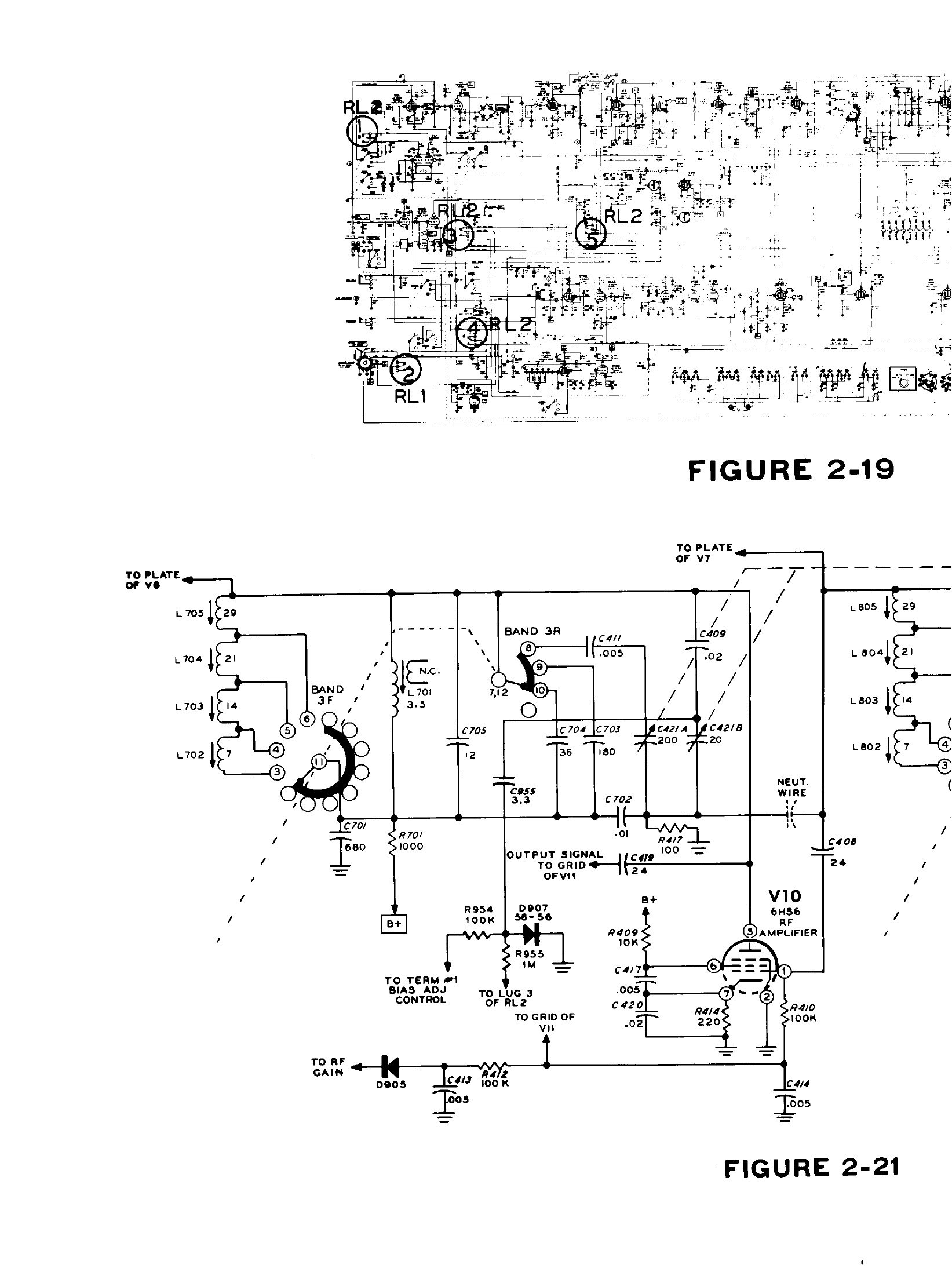
RF amplifier (V10, a 6HS6). The antenna relay feeds a link winding on L801 — the driver’s plate tank on transmit becomes the receiver’s input tuned circuit on receive — and V10’s own plate load is L701, the second transmitter mixer’s tank. The DRIVER PRESELECTOR therefore tunes the receiver front end and the transmitter driver with the same control and the same capacitors, which is elegant and which is also why the preselector must be re-peaked when the band is changed. Tube and stray capacitance differ between the two modes, so diode D907 switches an extra capacitor C955 into V10’s plate circuit on receive to make the preselector peak at the same dial setting in both directions.
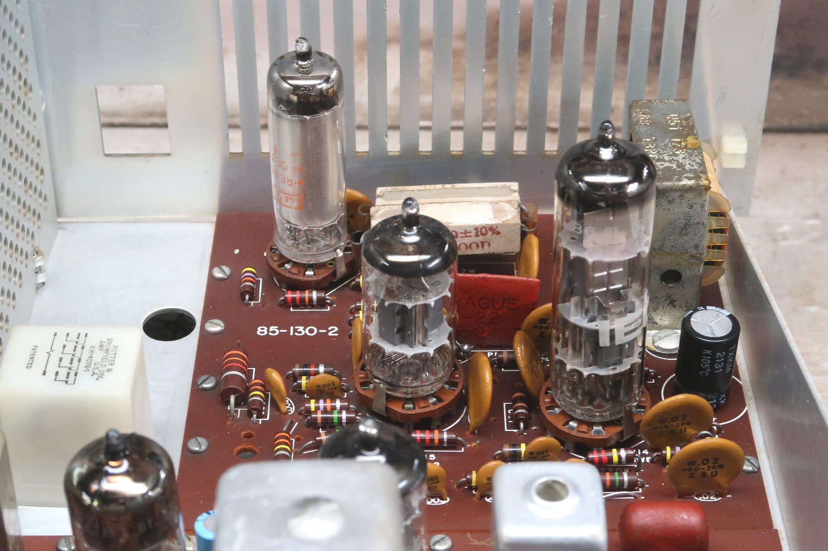
First receiver mixer (V11, a 6HS6) and second receiver mixer (V12A, half a 6EA8). V11 mixes the incoming signal with the heterodyne crystal down to the 8.395–8.895 MHz bandpass; V12A mixes that with the VFO down to the 3.395 MHz IF and into the crystal filter. Since both mixers use the same two oscillators as the transmitter, tuning is inherently transceive.
IF amplifiers (V3 and V4, both 6AU6) and AVC. V3 is the shared stage; V4 is receive-only and feeds the product detector through T103. Part of the IF signal is also taken to the AVC rectifiers in V13A and V13B, which develop a negative voltage proportional to signal strength across a two-capacitor network — one capacitor charging fast to catch peaks, the other slowly to follow the average. The result is the fast-attack, slow-release characteristic that SSB needs. That AVC voltage and the negative voltage from the RF GAIN control meet at a pair of diodes acting as a gate, so either can control the gain of V10, V11, V3 and V4 without one loading the other.
Product detector (V13C, a 6BN8) and audio. The 3.395 MHz IF meets the carrier oscillator’s output in V13C; the difference is audio. From the AF GAIN control it passes through V14A and the power stage V14B — the two halves of a 6GW8 — to output transformer T301, which offers a headphone tap and an 8 Ω speaker output rated at 2 watts. Negative feedback from the output back to V14B’s cathode keeps the distortion down.
2.4 Changing over: relays, VOX and anti-trip
Two relays do the switching, and the manual devotes a fold-out to what each set of contacts does. RL1 switches the antenna. RL2 does everything else: B+ to the screens of the transmit tubes in one position and to the receive tubes in the other, ALC voltage to V3 on transmit and AVC voltage to V3 on receive, cut-off bias grounded for whichever chain is meant to be running, and a spare set of contacts brought out to the accessory socket for keying an external linear (rated 3 A at 117 V AC).
Both relays are driven by V12B, the other half of the 6EA8 whose first half is the second receiver mixer. V12B is held cut off by a zener diode in its cathode; it conducts when a positive voltage appears at its grid, which happens either when the push-to-talk switch shorts its cathode to ground or when the VOX circuit rectifies speech. The VOX amplifier V17A takes audio from the speech amplifier, and D201 rectifies it; the VOX DELAY control sets how long capacitor C213 takes to discharge, and therefore how long the rig stays in transmit after the operator stops talking.
The anti-trip circuit stops the loudspeaker from keying the transmitter. Audio from the output stage is rectified into a negative voltage and fed to the same diode D201 as back bias, cancelling the VOX voltage that the speaker’s own output would otherwise produce. The ANTI-TRIP control sets how much — enough to cancel the speaker, not so much as to make the operator shout.
Transmit also mutes the receiver, and the manual is specific about how. A large negative bias, about −90 volts, is applied through the RF GAIN control and D905 to the grids of V10 and V11, hard enough to stop the transmitter’s own driver output from driving the RF amplifier into conduction on peaks. Smaller amounts cut off V12A, V4 and V14A. And a shaped negative pulse, formed by an RC network from the sudden plate-voltage change at V12B, cuts off the first audio stage before the relay contacts close, so that the operator does not hear the switching transient as a pop.
2.5 CW
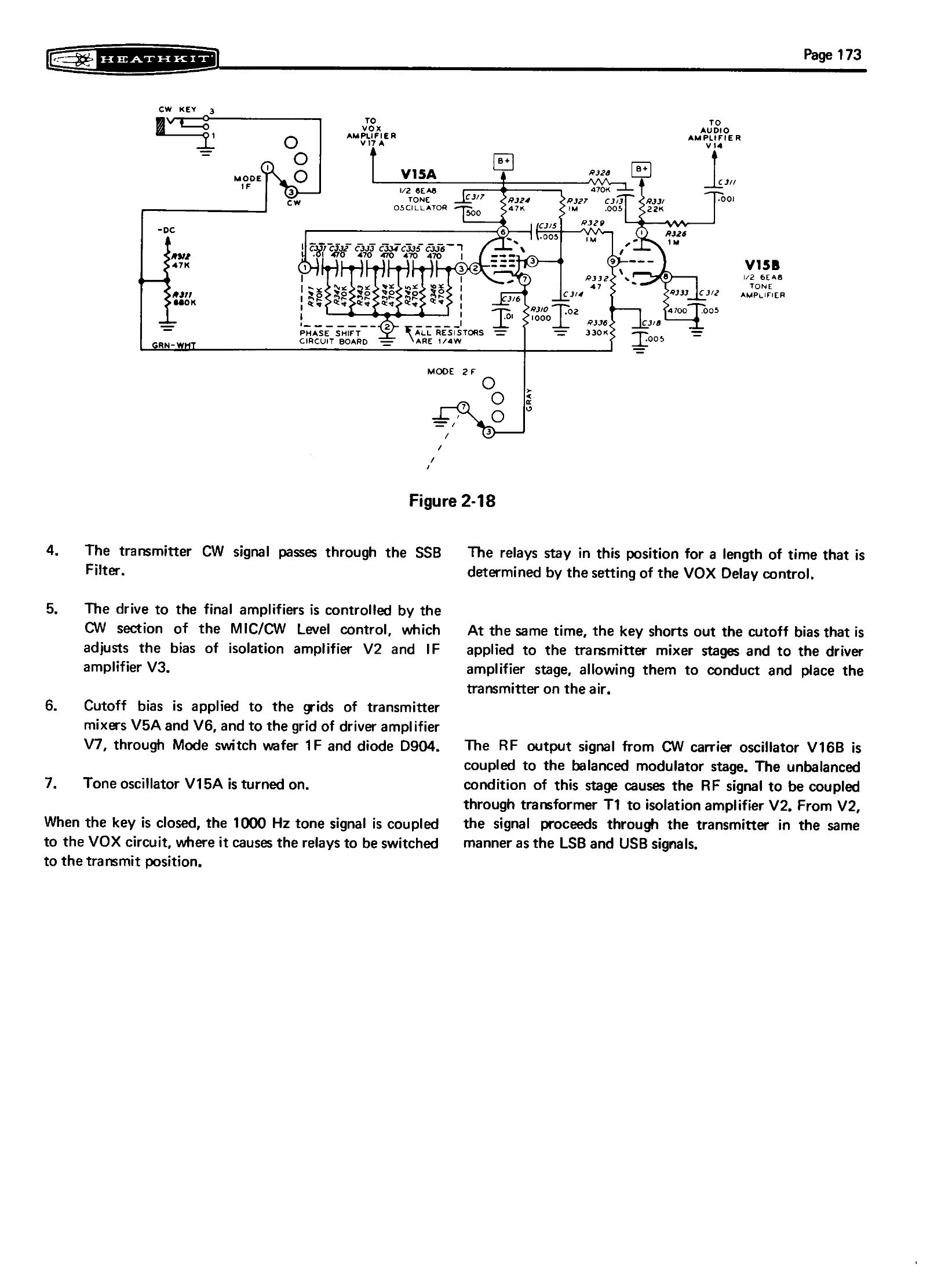
CW on a filter-type SSB rig is a set of small deceptions, and the HW-101’s are typical of the breed. Putting the mode switch to CW cuts off the cathode follower and grounds the VOX sensitivity control so that microphone noise cannot get in; connects crystal Y3 to the carrier oscillator; unbalances the diode ring so that it produces a carrier; applies cut-off bias to the two transmitter mixers and the driver; and turns on the tone oscillator V15A, half a 6EA8 running a phase-shift oscillator at about 1000 Hz.
Closing the key does two things at once. The 1000 Hz tone is coupled into the VOX circuit, which throws the relays; and the key shorts out the cut-off bias on the mixers and driver, letting them conduct. The same tone goes to the audio amplifier as a sidetone, so the operator monitors the keying. Break-in speed is therefore set by the VOX DELAY control, and the transmitted signal is a real carrier at the operating frequency rather than a tone somewhere in the passband.
Receiving CW uses the other half of the carrier oscillator. V16A and crystal Y1 act as a beat-frequency oscillator, and the offset between Y1 on receive and Y3 on transmit is arranged so that a station zero-beat against the transmitted frequency produces a 1000 Hz note in the speaker — the rig transmits on the frequency the operator hears at 1000 Hz, which is what makes calling a station on CW work without a receiver-incremental-tuning control.
2.6 Metering and regulation
The single meter reads four things. In transmit, the meter switch selects final cathode current (each numbered division on the scale represents 50 mA, so a reading of 9 means 150 mA and full scale at 60 means 300 mA), ALC voltage, or relative power taken from a diode sampling the output. In receive, the ALC position becomes the S-meter, because the same bridge across V3’s cathode and screen now follows AVC voltage instead of ALC. The ZERO ADJ control on the chassis sets the resting point with the antenna disconnected and the RF gain full up.
The OA2 gas regulator holds 150 volts for the oscillators, which is where the specified stability of under 100 Hz per hour comes from as much as from the VFO’s temperature compensation.
2.7 Numbering, and how to read the schematic
Heath’s designator scheme makes the schematic navigable without hunting, and it is worth learning before opening the fold-out. Every part number falls in a block that names its board:
Table 1 — Heath's designator scheme makes the schematic navigable without hunting, and it is worth learning before opening the fold-out. Every part number falls in a block that names its board
| Range | Board |
|---|---|
| 0–99 | Modulator circuit board |
| 100–199 | IF circuit board |
| 200–299 | Bandpass circuit board |
| 300–399 | Audio circuit board |
| 400–499 | RF driver circuit board |
| 500–599 | Crystal switch-board |
| 600–699 | Heterodyne oscillator switch-board |
| 700–799 | Driver grid switch-board |
| 800–899 | Driver plate switch-board |
| 900–999 | Chassis and VFO |
Rotary switches are named by their front-panel function plus a wafer number and an F or R for the front or rear face of that wafer, so “band switch wafer 5R” is an unambiguous physical location. Anyone tracing a fault in an HW-101 who knows that R202 is on the bandpass board and that L608 is on the heterodyne switch-board has already halved the work.
2.8 What the design costs and what it buys
Set against the SB-102 it was derived from, the HW-101 gives up the pre-built Linear Master Oscillator and the SB line’s finer dial mechanism, a little receiver performance, and some cosmetic polish. What it keeps is the whole frequency scheme, the same filter, the same finals and the same accessories. Set against a modern rig it gives up everything a synthesiser and a microprocessor buy: no receiver incremental tuning, no memories, no digital display, no general coverage, no click-free QSK. What it keeps is that every stage can be reached, measured and understood by one person with a meter, a signal generator and the manual — which is the property that has kept several thousand of them on the air.
Sources
- Heathkit Assembly Manual for the HW-101 SSB Transceiver, part 595-1277-18 (Heath Company, 1970), “Circuit Description”, pp. 161–181, and “Specifications”, pp. 157–160. Internet Archive
- HW-101 schematic, separately scanned. Internet Archive
- Cadman, Phil (G4JCP). “It’s a Classic! The Heathkit HW101.” Practical Wireless, November 2007. Scan
- Harris, Bill. “The Heathkit HW-101” — photographs of the boards and chassis of a restored unit. Link
- Eckweiler, Bob (AF6C). “Heathkit of the Month #30: The Amateur Radio SB-Line Overview” — for the LMO and the SB-line context. PDF
Comments (0)