ET-3400 Microprocessor Trainer · Volume 2
How It Works — the 6800, Memory, Display and Keypad
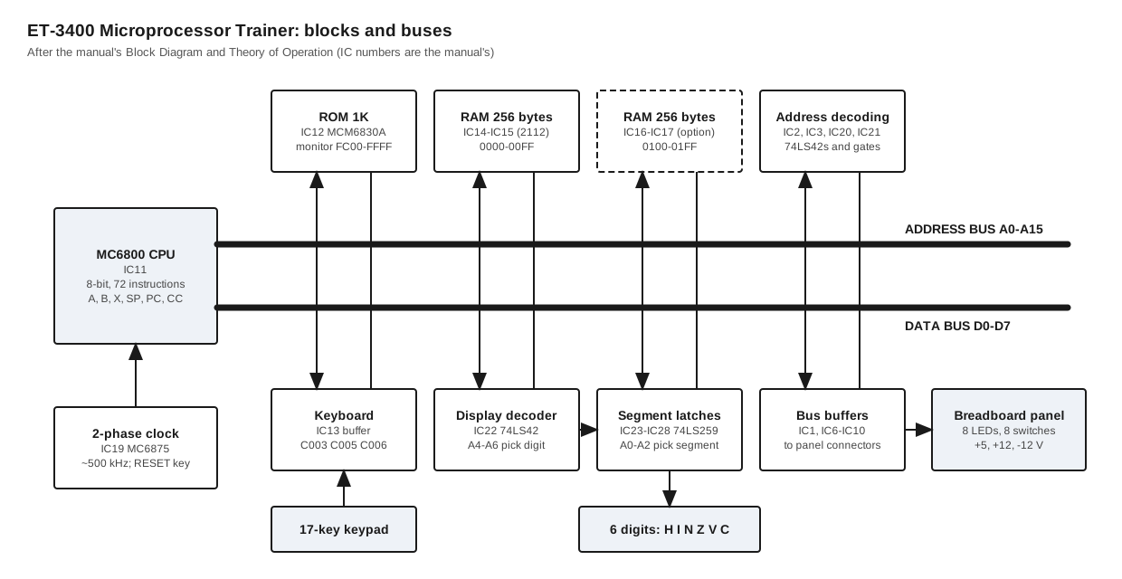
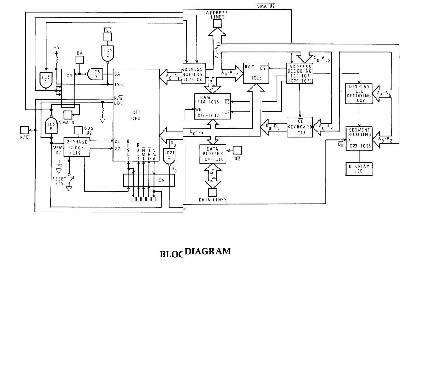
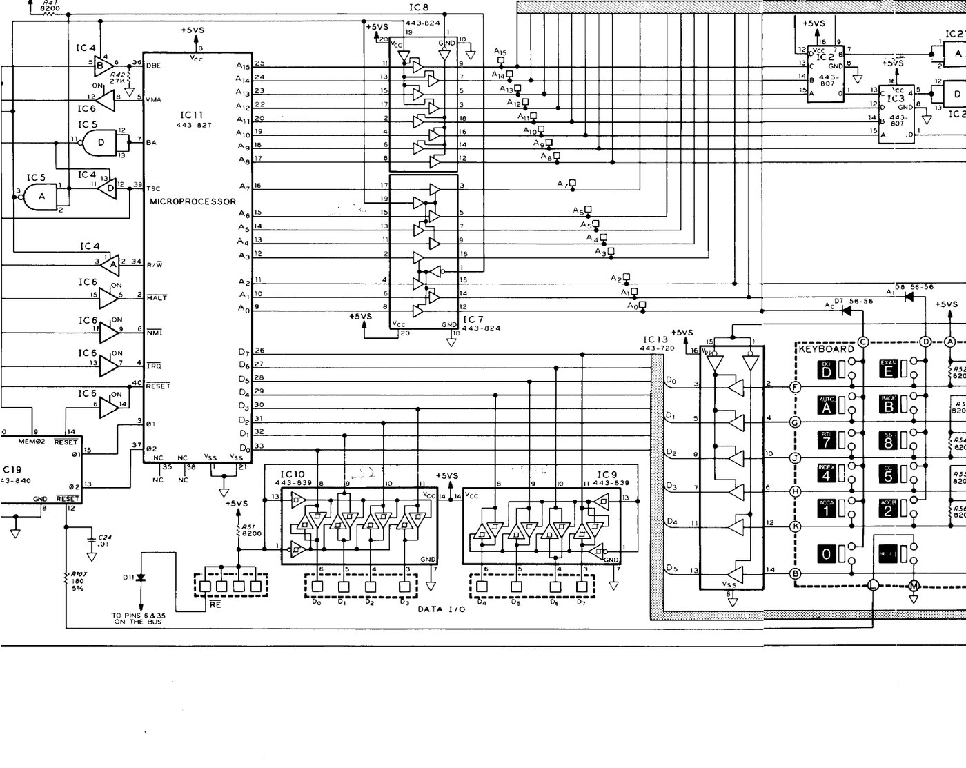
The ET-3400 is one circuit board, about 31 ICs, in which nearly everything is on the processor’s buses. There is no display controller, no keyboard encoder and no input/output chip. The six display digits are 48 one-bit latches that the processor writes like memory, and the keypad is a matrix of switches that it reads like memory. The 1K monitor program in ROM does the rest in software. That is why the trainer could be small, cheap and transparent: almost every part of it can be explained in terms of addresses, and the course did exactly that. This volume works through the block diagram, then the memory map, the display, the keypad, the breadboard section and the power supplies, using the manual’s own Theory of Operation and schematic (ET-3400 manual, 595-2021-03, pp. 87–88 and 108–109; illustration booklet in the 595-2021-06 printing).
2.1 The processor and its clock
The processor is a Motorola MC6800 (IC11, Heath part 443-827), the 8-bit NMOS microprocessor Motorola had introduced in 1974. To a programmer it has two 8-bit accumulators (A and B), a 16-bit index register (X), a 16-bit stack pointer, a 16-bit program counter, and a condition-code register with six flags: Half carry, Interrupt mask, Negative, Zero, oVerflow and Carry. The trainer’s six display digits are labelled H I N Z V C after those flags, and the monitor shows the condition-code register as six ones and zeros, one under each letter (manual, p. 46).
The 6800 needs two non-overlapping clock phases, φ1 and φ2, which it does not make itself. The ET-3400 uses Motorola’s MC6875 clock generator (IC19, part 443-840). The manual gives the clock as “500 kHz (approximately)”, and the course’s own one-second delay routines exist in two versions: “The original trainer has a clock frequency of approximately 500 kHz”, while a trainer “modified for use with the Heathkit Memory I/O Accessory ETA-3400 … has a clock frequency of 1 MHz” (manual, p. 107; Microprocessors, EB-6401A, Experiment 8 discussion). At 500 kHz one machine cycle takes 2 µs; the shortest instructions take two cycles and the longest, a software interrupt, twelve.
The MC6875 also produces a clean reset pulse. The keypad’s RESET key is wired to the clock chip, not to the keyboard matrix; the chip’s reset output goes through a tri-state buffer (IC6) to the CPU’s reset pin (manual, p. 108). Pressing RESET makes the 6800 fetch its reset vector from FFFE–FFFF, which points to the monitor at FC00.
The processor’s control lines are buffered and brought to the panel. VMA (valid memory address) is NANDed with the memory clock φ2 to make VMA·φ2, the strobe that enables all the address decoders, so nothing is selected during the cycles in which the 6800 puts meaningless addresses on the bus. BA (bus available) and TSC (three-state control) let an experiment take the buses away from the processor; the manual explains how pulling TSC high tri-states the address buffers, R/W, DBE and VMA·φ2 (manual, p. 108). These lines are the reason the trainer could teach direct memory access and multiprocessor ideas, not only programming.
2.2 The memory map
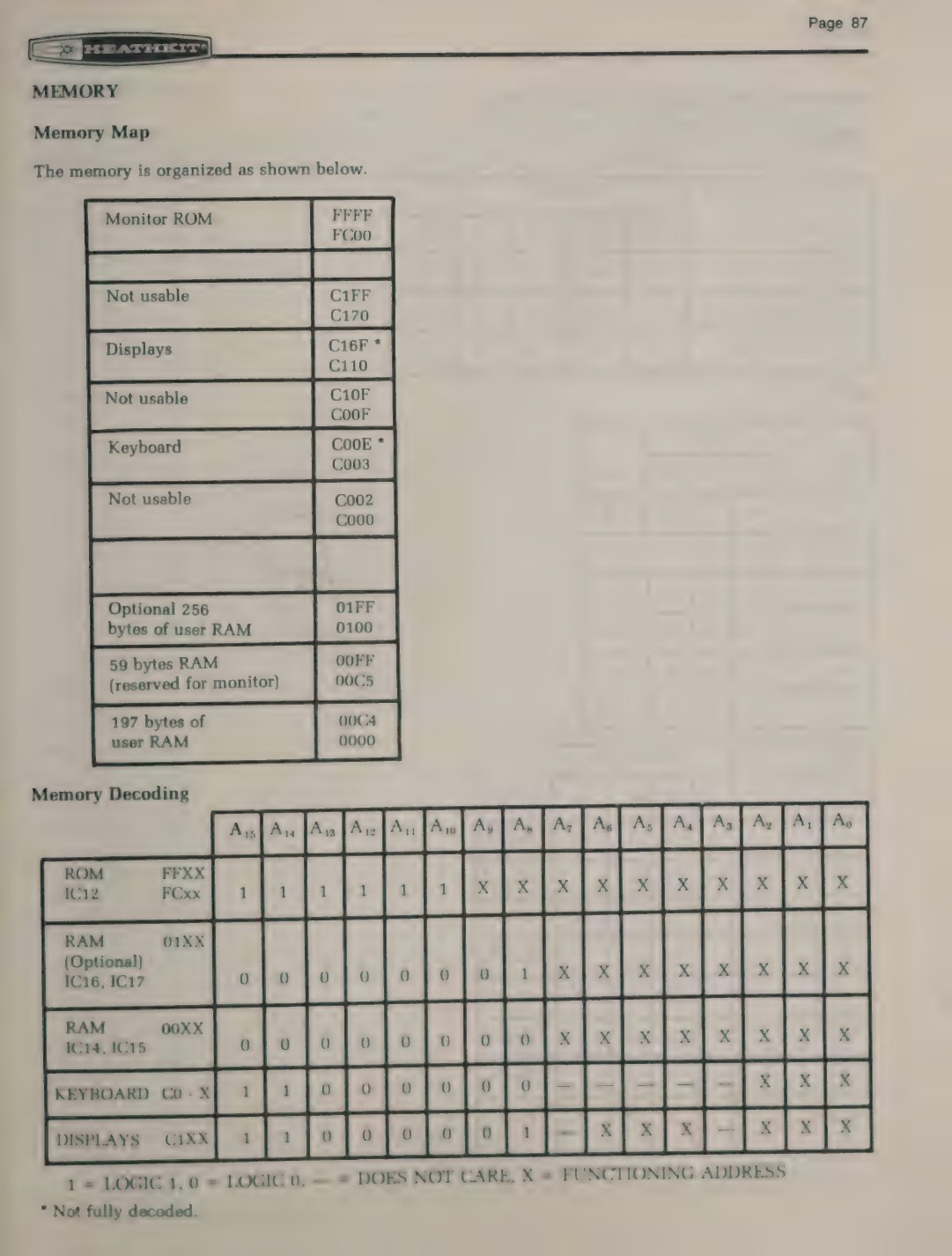
The trainer decodes only what it needs. The manual’s memory map and decoding table show five regions in the 64K address space (manual, p. 87):
Table 1 — The trainer decodes only what it needs. The manual's memory map and decoding table show five regions in the 64K address space ([manual, p. 87](https://archive.org/details/manualsplus11737))
| Addresses | What | Decoded by |
|---|---|---|
| 0000–00FF | 256 bytes of RAM (IC14, IC15); 0000–00C4 for the user, 00C5–00FF reserved for the monitor | high byte 00 |
| 0100–01FF | optional 256 bytes of RAM (IC16, IC17), supplied with the EE-3401 course | high byte 01 |
| C003–C00E | keyboard (not fully decoded) | high byte C0 |
| C110–C16F | display latches (not fully decoded) | high byte C1 |
| FC00–FFFF | 1K monitor ROM (IC12) | high bytes FC–FF |
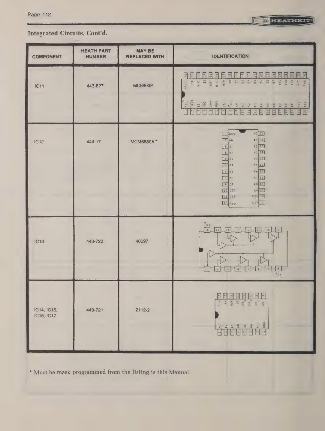
Each RAM bank is a pair of Intel-type 2112 static RAMs (part 443-721), each 256 words by 4 bits; one chip holds the low four bits of every byte and the other the high four. The ROM is a Motorola MCM6830A (part 444-17), a 1024-byte mask-programmed ROM; the parts table notes that a replacement “must be mask programmed from the listing in this Manual” (manual, p. 112). The address decoders are 74LS42 BCD-to-decimal decoders (IC2, IC3, IC20, IC22) with 74S00 gates.
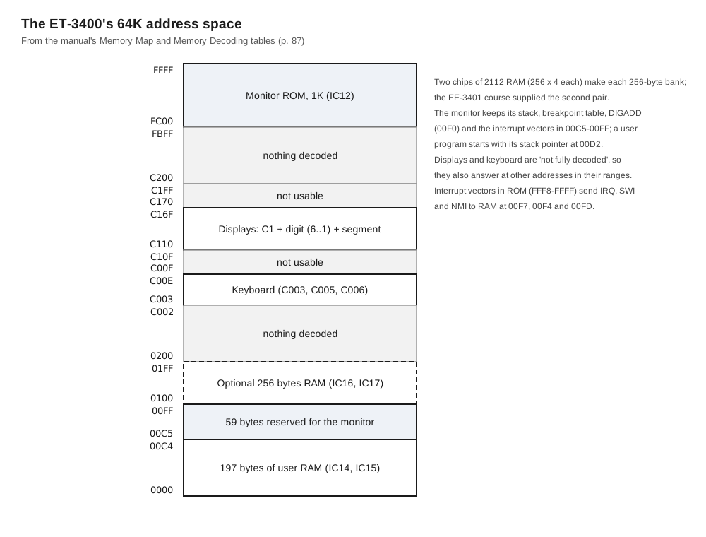
The 59 reserved bytes hold the monitor’s working storage. The listing’s table of “reserved memory bytes in RAM” names them: a user stack area, the monitor’s stack, a breakpoint table (four entries), temporary storage, DIGADD at 00F0 (the address of the next display digit), the saved user stack pointer at 00F2, and three-byte jump vectors at 00F4 (system SWI), 00F7 (user IRQ), 00FA (user SWI) and 00FD (user NMI) (manual, p. 86). The ROM’s interrupt vectors point into these RAM locations, so a student can attach an interrupt routine by writing a JMP into RAM without changing the ROM. A user program starts with the stack pointer at 00D2 (manual, p. 52).
2.3 The display: 48 latches
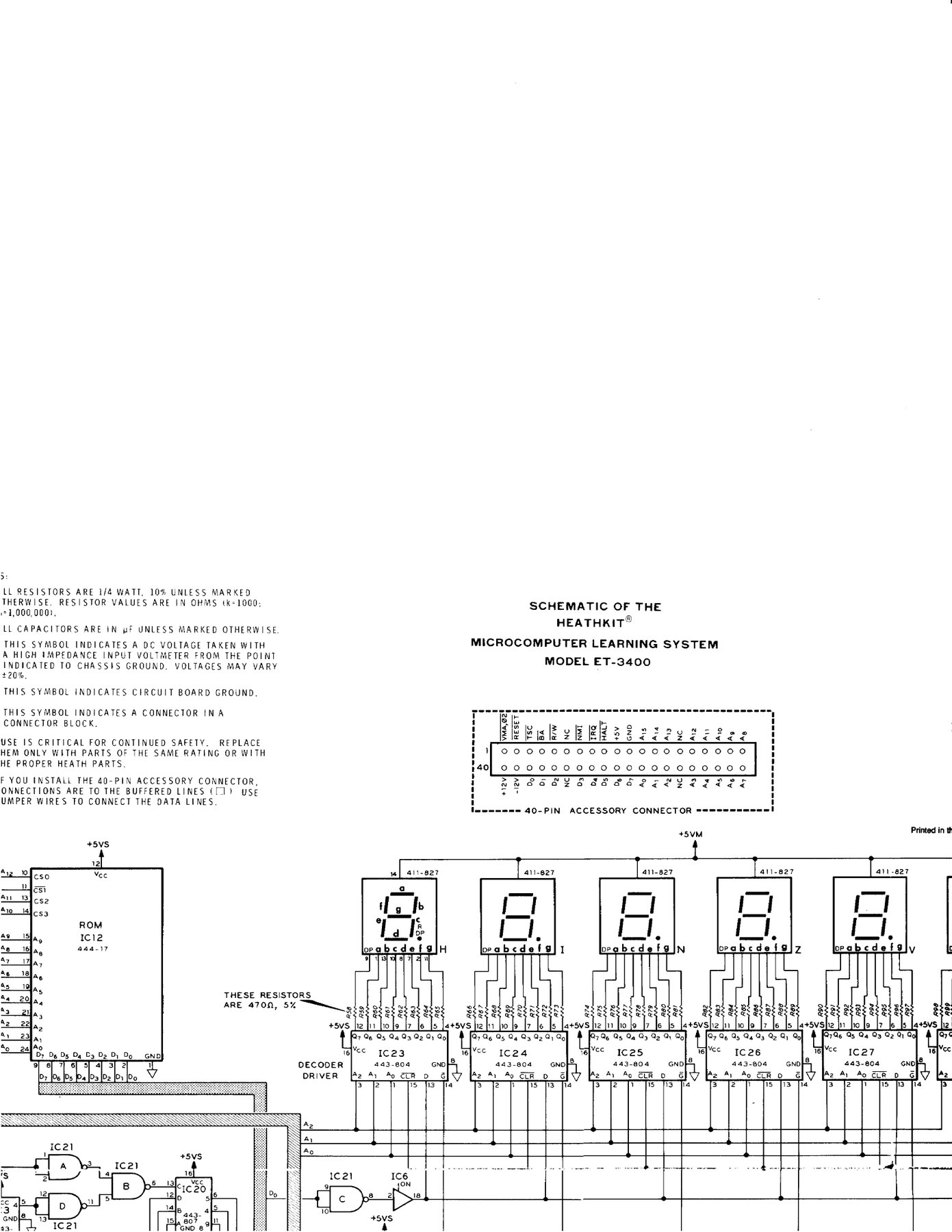
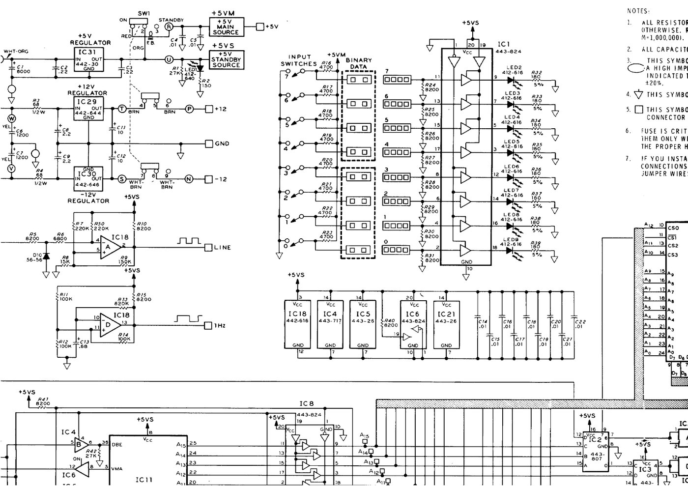
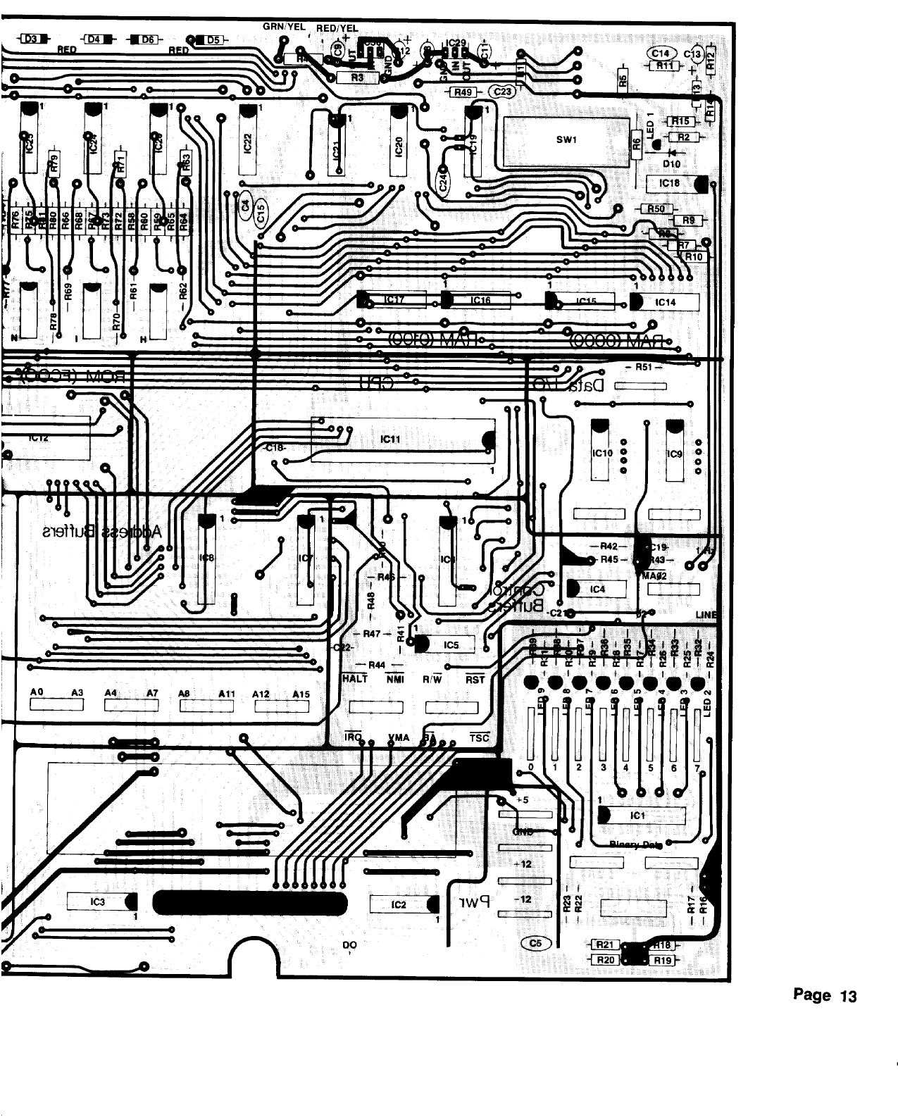
The display is the trainer’s most instructive circuit. There is no character generator and no multiplexing. Each of the six digits has its own 74LS259 eight-bit addressable latch (IC23–IC28, part 443-804), one bit per segment and one for the decimal point, and each latch output drives one segment of a common-anode TIL312 LED digit through a current-limiting resistor (manual, pp. 109–111).
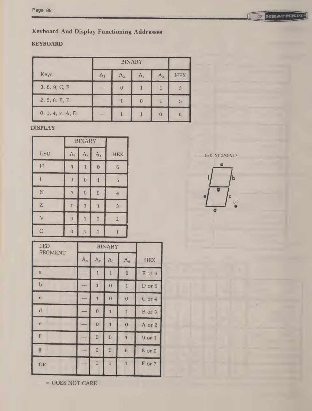
The processor reaches a segment through its address. When the high byte is C1, a decoder places a logic 0 on the D input of IC22, a 74LS42. Address lines A6, A5 and A4 then select one of its outputs 1 to 6, which enable the six latch drivers: “A hex 6 or BCD 110 on lines A6, A5, and A4 will cause the enable line for the left-most latch driver (IC23 and DISPLAY LED H) to be logic 0” (manual, p. 109). Address lines A2, A1 and A0 go to the latch-select inputs of all six latches and choose one of the eight bits. The data comes from a single bus line, D0, inverted by IC21C. A 1 on D0 therefore lights the addressed segment and a 0 turns it off, and the latch holds the state until it is written again.
So the H display’s decimal point is address C16F (or C167, since A3 is not decoded), its top segment C16E, and so on down to the middle segment at C168. The rightmost digit, C, is C11F to C118. The manual’s operational test has the builder prove this before the monitor is ever used: a three-instruction program stores 01 at C16F, and the H decimal point lights (manual, pp. 38–41).
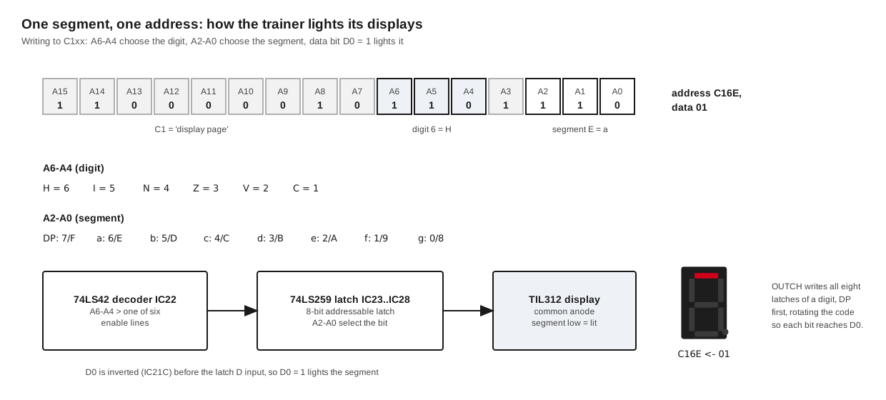
The cost of this design is software. To show a character, the program must write eight separate addresses. The monitor’s OUTCH routine does it in a loop, and its trick is worth reading in the listing. It takes a byte whose bit 7 is the decimal point and bits 6 to 0 are segments a to g, rotates it through the carry flag, and stores the accumulator at each of the digit’s latch addresses in turn, counting the address down; because only D0 matters to the latch, each store delivers one bit. It makes sixteen passes rather than eight (the comment reads “two passes at lighting digits — King’s X on first pass”) so that after nine-bit rotation the accumulator and carry come back to where they started, and it leaves DIGADD pointing at the next digit to the right (manual, monitor listing, p. 81). Volume 5 uses this routine, and the emulator reproduces its effect.
There is one more path to the displays. Two pins at the right edge of the board marked SEGMENT TEST, when shorted, light every segment and decimal point of every digit, a hardware test that does not need the processor (manual, p. 34).
2.4 The keypad: a matrix read like memory
The 16 hex keys sit in three columns. Reading address C006 pulls the column with keys 0, 1, 4, 7, A and D low; C005 pulls the column with 2, 5, 8, B and E; C003 the column with 3, 6, 9, C and F. A closed key in the selected column pulls one data line low, and a CMOS buffer (IC13, a 40097) puts the result on the bus. “Which key is closed is determined by the monitor program by knowing the address that is on the line and which data line is 0.” Diodes in series with the three address lines stop two pressed keys from shorting adjacent columns together (manual, pp. 88 and 108).
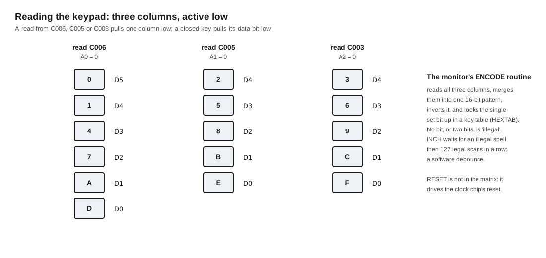
The monitor turns this into key values in two layers. ENCODE reads the three columns, packs them into a 16-bit pattern, inverts it, and looks for exactly one set bit; no bit or two bits is “illegal” and clears the carry flag. INCH builds a debounce out of ENCODE: it waits until ENCODE has reported an illegal state (no key) for 127 scans in a row, then until it has reported the same legal key for 127 scans in a row. The listing’s comments are in a prison idiom: the counters are “violation count” and “time until parole”, and a failed count is “back in the slammer” (manual, pp. 79–80).
The keys are dual-function. After RESET the display shows CPU UP, and the next key is a command: 0 is not used as a command, 1 ACCA, 2 ACCB, 3 PC, 4 INDEX, 5 CC, 6 SP, 7 RTI (resume), 8 SS (single step), 9 BR (set breakpoint), A AUTO, B BACK, C CHAN (change), D DO, E EXAM, F FWD. The order follows the monitor’s command table, CMDTAB, at FFB6 (manual, pp. 45–48 and 85). Volume 4 describes how they are used.
2.5 The monitor
The 1K monitor is the trainer’s operating system. The listing in the manual ends with “STATEMENTS = 970 … NO ERRORS DETECTED” and is the complete source, with comments (manual, pp. 73–85). It provides:
- Reset and main loop. RESET loads the monitor’s stack pointer, prints CPU UP, sets up a user register frame and clears the breakpoint table; MAIN then reads a key with INCH and jumps through CMDTAB.
- Register and memory display (REGA, REGB, REGP, REGX, CONDX, STKPTR, MEM), memory change (REPLAC, AUTO, FWD, BACK) and address entry with prompts.
- Breakpoints. BR stores up to four addresses; when the program is resumed, the monitor saves the op code at each one and replaces it with SWI (3F). When the program reaches one, the SWI returns control to the monitor, which restores the op codes and shows the address and instruction.
- Single step. SS executes one instruction. Because the 6800 has no hardware trace, the monitor does it in software: a table of legal op codes, OPTAB, tells it how long the instruction is, and special handlers (BSRH, JSRH, RTSH, JMPH and others) work out where branches, jumps and returns go, so the monitor can plant a breakpoint after the instruction and run it. An invalid op code is refused: “the single step routine will not execute an invalid instruction and the display will not change” (manual, p. 51).
- Display and keyboard subroutines for user programs: REDIS, OUTCH, OUTHEX, OUTBYT, OUTSTR and its variants, DSPLAY, ENCODE, INCH and IHB. Volume 5 lists their entry points and uses them.
The manual’s warning about breakpoints shows how close to the machine the student was. A breakpoint placed on an operand byte instead of an op code turns data into 3F; the program then “crashes”, and “the display will be blank; all eights will be displayed; or all eights will appear, followed by CPU UP” (manual, p. 51). The fix was to press RESET, examine memory, and put the right bytes back.
2.6 The breadboard section
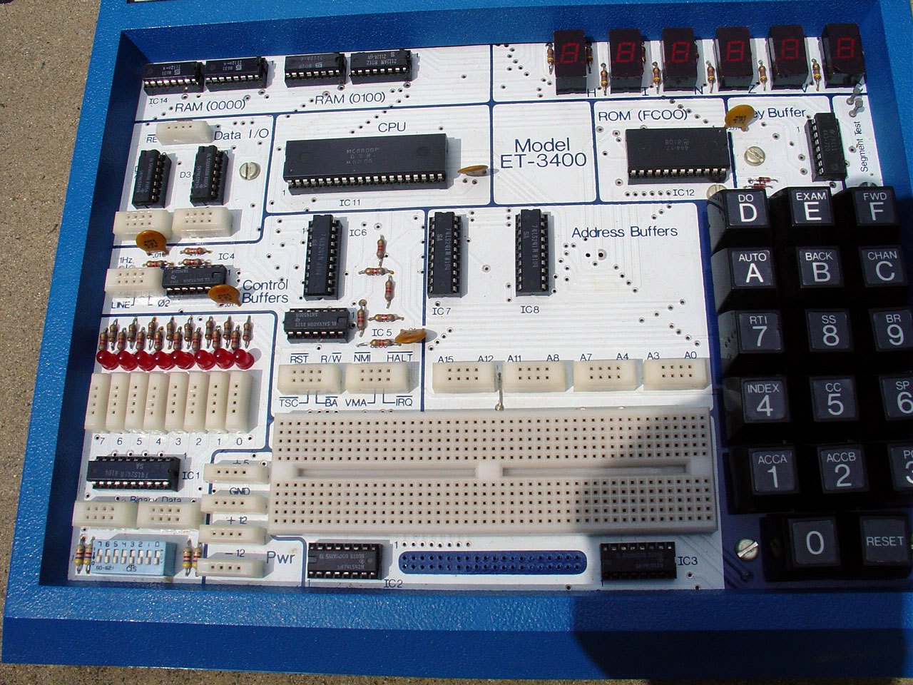
The lower left of the board is a digital trainer like the ET-3200, with the processor’s lines next to it.
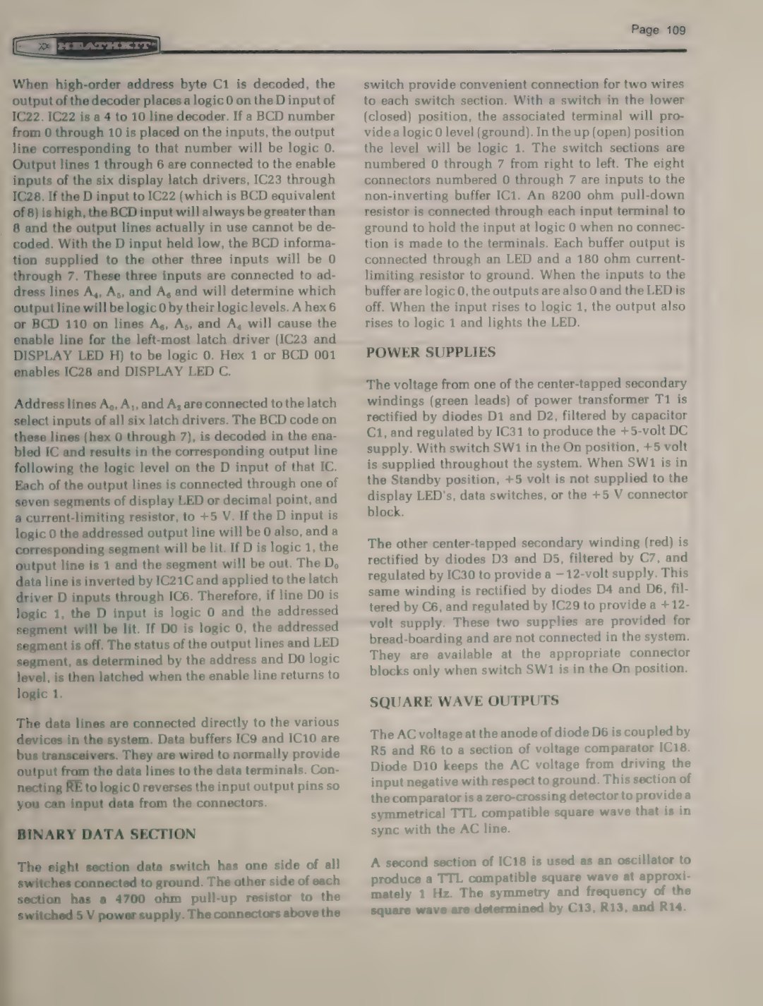
- Eight data switches in a DIP package. One side of each is grounded; the other has a 4700 Ω pull-up to the switched +5 V and goes to two terminals. A closed switch gives a logic 0 and an open one a logic 1. They are numbered 0 to 7 from right to left (manual, p. 109).
- Eight logic LEDs with their own input terminals, driven through a non-inverting 74LS241 buffer (IC1). An 8200 Ω pull-down holds an unconnected input at 0, and each buffer output lights its LED through a 180 Ω resistor.
- Buffered buses. The address lines go out through 74LS241 buffers (IC7, IC8). The data lines go through 74LS243 bus transceivers (IC9, IC10) that normally drive the terminals; pulling the line marked RE low reverses them, so an experiment can put data onto the bus, for example from an input port the student has built (manual, p. 109).
- Square-wave sources. A section of an LM3302 comparator (IC18) acts as a zero-crossing detector on the transformer’s secondary and gives a TTL square wave synchronised with the mains; a second section runs as an oscillator at about 1 Hz, set by C13, R13 and R14 (manual, p. 109). The φ2 and VMA·φ2 clocks are on terminals too. (The ET-3200 dive’s volume 5 says the ET-3400 dropped the ET-3200’s line-frequency source; the ET-3400 manual shows that it kept one, plus a 1 Hz source.)
- A 40-pin connector position between IC2 and IC3 for “extending memory and I/O”. The kit did not include the connector; the manual names suitable parts from AP Products, Molex and AMP and tells the builder to wire eight jumpers from the connector’s data pins to the data bus (manual, p. 41). The ETA-3400 accessory later plugged in here.
2.7 Power supplies
The power transformer has two centre-tapped secondary windings. One, through diodes D1 and D2 and filter capacitor C1, feeds IC31, a µA309K five-volt regulator in a TO-3 case (part 442-30), which supplies the logic and the +5 V terminal: 1.5 A in all, 0.5 A of it available at the breadboard. The other winding, rectified by D3 to D6, feeds two small regulators, an LM78L12 (IC29) for +12 V and an LM79L12AC (IC30) for −12 V, each rated 50 mA at the terminals. The ±12 V rails “are provided for breadboarding and are not connected in the system” (manual, pp. 107 and 109).
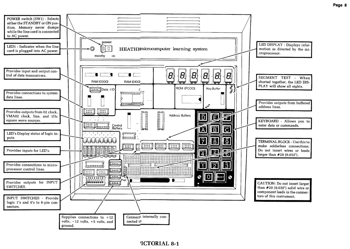
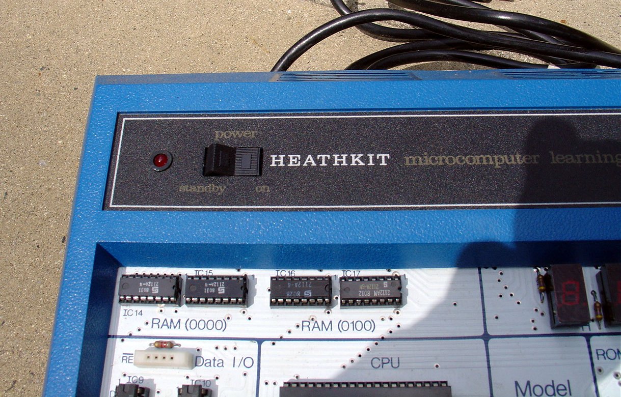
The power switch has a third state that matters to a programmer. In Standby, +5 V stays on the processor and memory but is removed from the displays, the data switches and the +5 V terminal, and the ±12 V rails are off. A program entered by hand survives as long as the trainer stays plugged in: the panel guide puts it as “memory never dumps while the line cord is connected to AC power”. A red LED beside the switch is lit whenever the cord is plugged in, whatever the switch position (manual, pp. 34 and 109; Pictorial 8-1).
2.8 The parts, and why they were chosen
Table 2 — The parts, and why they were chosen
| IC | Part | Heath no. | Job |
|---|---|---|---|
| IC11 | MC6800P | 443-827 | processor |
| IC19 | MC6875 | 443-840 | two-phase clock and reset |
| IC12 | MCM6830A (mask ROM) | 444-17 | 1K monitor |
| IC14–IC17 | 2112-2 | 443-721 | 256 × 4 static RAM (four fitted with the course RAM) |
| IC1, IC6, IC7, IC8 | 74LS241 | 443-824 | LED driver and bus buffers |
| IC9, IC10 | 74LS243 | 443-839 | data bus transceivers |
| IC2, IC3, IC20, IC22 | 74LS42 | 443-807 | address and digit decoding |
| IC4 | 74126 | 443-717 | tri-state control buffers |
| IC5, IC21 | 74S00 | 443-26 | gating, D0 inversion |
| IC13 | 40097 | 443-720 | keyboard buffer |
| IC23–IC28 | 74LS259 | 443-804 | display latches |
| IC18 | LM3302N (or LM2901N, µA775, selected) | 442-616 | line and 1 Hz square waves |
| IC29, IC30, IC31 | LM78L12, LM79L12AC, µA309K | 442-644, 442-646, 442-30 | +12, −12 and +5 V regulators |
| H, I, N, Z, V, C | TIL312 | 411-831 | common-anode seven-segment digits |
Source: manual, Semiconductor Identification Charts, pp. 110–113.
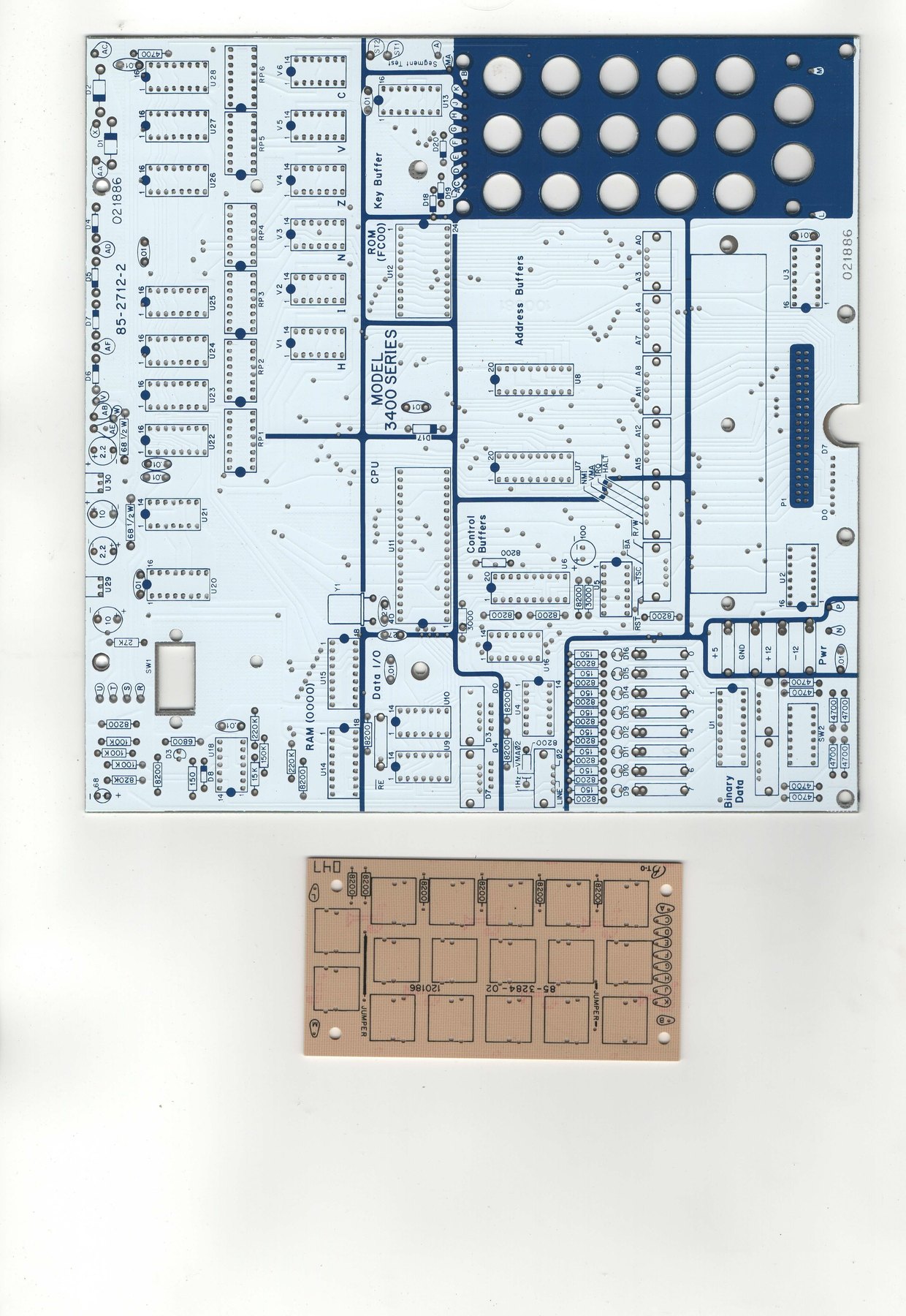
Almost every choice favours visibility over economy. Static RAM needs no refresh circuit to explain. Latched, unmultiplexed displays keep their state when the processor is stopped at a breakpoint, so a single-stepping student sees exactly what the last store did. Segment addressing makes the display a lesson in address decoding rather than a black box. A Motorola part list (processor, clock, ROM) kept the course in one family, and the 6800 family stayed: the ET-3400A changed to the 6808, which carries its own oscillator and drives it from a crystal (Microprocessors, EB-6401A, Introduction). The later boards also changed part numbers: Herb Johnson’s ET-3400A carries boards 85-2010 and 85-2712 and a 1981 date code on its chips (retrotechnology.com). No ET-3400A schematic or manual was found to document the rest of the revision.
Sources
- Heath Company. Heathkit Manual for the Microprocessor Trainer, Model ET-3400, 595-2021-03, © 1977. Internet Archive (DLARC). https://archive.org/details/manualsplus_11737
- Heath Company. Same manual, 595-2021-06 printing (c. 1980), with the Illustration Booklet and schematic. Internet Archive. https://archive.org/details/HeathkitManualForTheEt-3400MicroprocessorTrainer
- Heathkit Educational Systems. Microprocessors, EB-6401A, © 1978, 1985. https://archive.org/details/6800-Microprocessors-Book-1and-2-Heathkit-1985
- Johnson, Herb. “Heathkit ET-3400A 6800.” https://www.retrotechnology.com/restore/et3400A.html
- Internet Archive, “et3400-a scans.” https://archive.org/details/et3400-a-scans
- DigiBarn Computer Museum. https://www.digibarn.com/collections/systems/heathkit-microprocessor-learning-kit/
Comments (0)